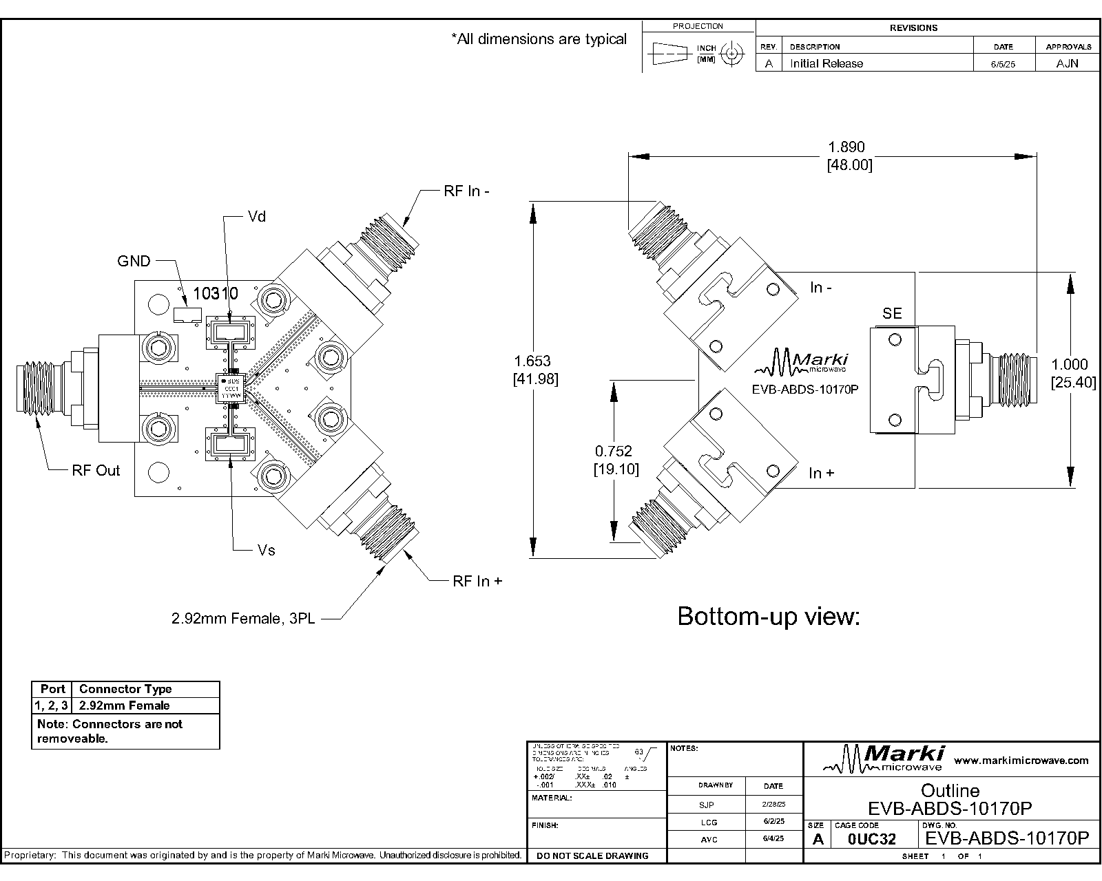
Port Diagram
Below is the port diagram for the ABDS-10170PSM. The diagram is shown as an x-ray view from the top down.

Sales: 408-778-9952 | General: 408-778-4200 | Fax: 408-778-4300
Sales & Customer Support: [email protected]
Tech Support: [email protected]
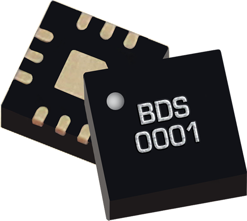
The ABDS-10170PSM is a GaAs active MMIC balun in a 3mm QFN surface mount package. It offers 3 dB differential to single ended gain from low frequencies (limited by DC block) to 30 GHz. The 3mm QFN package is a lead free, RoHS compliant package compatible with standard leaded and lead-free solder reflows. Connectorized evaluation packages are available. The ABDS-10170PSM is an excellent choice for converting digital to analog converter differential outputs to single ended.

| Part Number | Description | Package | Green Status | Product Lifecycle | Export Classification |
|---|---|---|---|---|---|
| ABDS-10170PSM | 30 GHz Differential to Single Ended Active Balun | QFN | REACH RoHS | Released | EAR99 |
| EVB-ABDS-10170P | Evaluation Board | EVB | REACH RoHS | Released | EAR99 |
ABDS-10170PSM
30 GHz Differential to Single Ended Active Balun
| Revision Code | Revision Date | Comment |
|---|---|---|
| - | 2025-06-24 | Initial Release |
ABDS-10170PSM
30 GHz Differential to Single Ended Active Balun
Below is the port diagram for the ABDS-10170PSM. The diagram is shown as an x-ray view from the top down.
ABDS-10170PSM
30 GHz Differential to Single Ended Active Balun
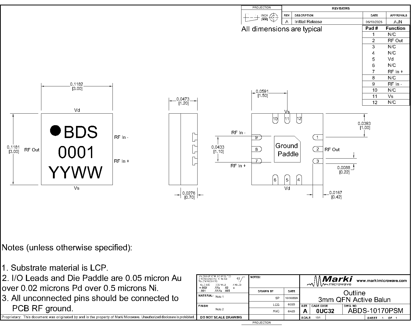
| Port | Function | Description | DC Equivalent Circuit |
|---|---|---|---|
| 11 | Vs | Pin 11 is the negative DC supply voltage for the device. | - |
| 1,3,4,6,8,10 and 12 | Non-connect (NC) | These pins are not connected internally. Datasheet performance is tested with NC pins grounded. | - |
| 2 | RF Output | Pin 2 is the RF output of the device. This pin is internally RF matched to 50 Ohms and is DC coupled. This pin requires an external DC blocking capacitor if DC is present on the input line. If the line is DC ground or floating, an external DC blocking capacitor is unnecessary. | - |
| 5 | Vd | Pin 5 is the positive DC supply voltage for the device. | - |
| 7 | RF In + | Pin 7 is the positive RF input of the device. This pin is internally RF matched to 50 Ohms and is DC coupled. This pin requires an external DC blocking capacitor. | - |
| 9 | RF In - | Pin 9 is the negative RF input of the device. This pin is internally RF matched to 50 Ohms and is DC coupled. This pin requires an external DC blocking capacitor. | - |
| Paddle | Ground | Ground pad should be connected to RF/DC ground with low electrical and thermal resistance. | - |
ABDS-10170PSM
30 GHz Differential to Single Ended Active Balun
The Absolute Maximum Ratings indicate limits beyond which damage may occur to the device. If these limits are exceeded, the device may be inoperable or have a reduced lifetime. This device is designed and characterized in a 50Ω system (100Ω differential output), and operation in a reflective environment can cause performance degradation.
| Parameter | Maximum Rating | Unit |
|---|---|---|
| Drain Current (Id) (No RF Applied) 1 | 84 | mA |
| Maximum Operating Temperature | 85 | °C |
| Maximum Storage Temperature | 150 | °C |
| Minimum Operating Temperature | -40 | °C |
| Minimum Storage Temperature | -65 | °C |
| RF Input Power | 10 | dBm |
| Source Current (Is) no RF applied | -84 | mA |
| Total DC Supply Voltage (Vd-Vs) | 9.5 | V |
[1] Max current density across TFR
| Parameter | Details | Rating |
|---|---|---|
| ESD | < 50 Volts | HBM 0Z |
| Dimensions | - | 3 x 3 mm |
| Moisture Sensitivity Level | - | MSL 1 |
| Parameter | Min | Nominal | Max | Unit |
|---|---|---|---|---|
| Negative DC Voltage (Vs) | -3 | -4 | -4 | V |
| Positive DC Voltage (Vd) | 3 | 4 | 4 | V |
| Negative DC Current (Is) (No RF Input) | -67 | -67 | -50 | mA |
| Positive DC Current (Id) (No RF Input) | 50 | 67 | 67 | mA |
ABDS-10170PSM
30 GHz Differential to Single Ended Active Balun
Specifications guaranteed for +25°C, measured in a 50Ω system. Measured data was taken on an evaluation board and de-embedded to surface mount launch unless otherwise noted.
| Parameter | Test Conditions | Minimum Frequency (GHz) | Maximum Frequency (GHz) | Min | Typ | Max | Unit |
|---|---|---|---|---|---|---|---|
| Single-Ended Gain | Vd=4V, Vs=-4V | 0 | 30 | - | -1.5 | - | dB |
| Output IP3 1 | Vd=4V, Vs=-4V | 0 | 30 | - | 18 | - | dBm |
| Common Mode Rejection | Vd=4V, Vs=-4V | 0 | 30 | - | 33 | - | dB |
| Impedance Ratio | - | - | - | - | 2:1 | - | - |
| Amplitude Balance | Vd=4V, Vs=-4V | 0 | 30 | - | 0.2 | - | dB |
| DC Supply Quiescent Current (Idq) | Vd=4V, Vs=-4V | - | - | - | 67 | - | mA |
| Differential Power Gain | Vd=4V, Vs=-4V | 0 | 30 | - | 1.5 | - | dB |
| HD2 | Vd=4V, Vs=-4V, differential input power=0dBm | 0 | 15 | - | 48 | - | dBc |
| HD3 | Vd=4V, Vs=-4V, differential input power=0dBm | 0 | 15 | - | 44 | - | dBc |
| Input Return Loss | Vd=4V, Vs=-4V | 0 | 30 | - | 22 | - | dB |
| Noise Figure 2 | Vd=4V, Vs=-4V | 0.1 | 30 | - | 8.2 | - | dB |
| Nominal Phase Shift 3 | Vd=4V, Vs=-4V | 0 | 30 | - | 180 | - | ° |
| Output IP2 4 | Vd=4V, Vs=-4V | 0 | 15 | - | 50 | - | dBm |
| Output Return Loss | Vd=4V, Vs=-4V | 0 | 30 | - | 23 | - | dB |
| Phase Balance 5 | Vd=4V, Vs=-4V | 0 | 30 | - | 2 | - | ° |
| Reverse Isolation | Vd=4V, Vs=-4V | 0 | 30 | - | 37 | - | dB |
[1][4] Measured with 10MHz offset differential tones at input, differential input power=-7dBm per tone
[2] Measured using a balun at the input to produce a differential signal. The external balun and associated losses are de-embedded from the measurement. EVB trace and connector losses are still present in the data.
[3][5] Measured single-ended with connector and evb effects de-embedded.
ABDS-10170PSM
30 GHz Differential to Single Ended Active Balun
Three-port scattering parameters measured as three single-ended 50Ω ports unless otherwise noted. Small signal gain, return losses and reverse isolation have evb and connector effects de-embedded.


ABDS-10170PSM
30 GHz Differential to Single Ended Active Balun
Measurements are with 50-Ω single-ended input, and 100-Ω differential output. EVB and connector effects are included in these measurements. All plots are with respect to input frequency.


ABDS-10170PSM
30 GHz Differential to Single Ended Active Balun
Measured differentially and includes EVB and connector noise contributions.


ABDS-10170PSM
30 GHz Differential to Single Ended Active Balun
Mixed mode scattering parameters are used to characterize differential circuits. For baluns, this means that the 0° and 180° ports become a single 100Ω differential port and the common port remains the same 50Ω common port. The two-port s-parameters of the balun are then characterized based on differential (d), common mode (c), or single-ended (s) signals. For example: Sds12 is the single ended to differential reverse isolation of the active balun. Sdc11 is the return loss measured as ratio of differential reflect to common mode incident signal on the input port.


ABDS-10170PSM
30 GHz Differential to Single Ended Active Balun

ABDS-10170PSM
30 GHz Differential to Single Ended Active Balun
ABDS-10170PSM
30 GHz Differential to Single Ended Active Balun
Download : Footprint Drawing

ABDS-10170PSM
30 GHz Differential to Single Ended Active Balun