| Parameter | Typ | Unit |
|---|---|---|
| Frequency Range | 0 to 50 | GHz |
| Attenuation | 4.75 | dB |
| Return Loss | 20 | dB |
Summary only – refer to the Electrical Specifications, Absolute Maximum Ratings, and Recommended Operating Range tables for complete details.

Sales: 408-778-9952 | General: 408-778-4200 | Fax: 408-778-4300
Sales & Customer Support: [email protected]
Tech Support: [email protected]
ATN06-0050CSP1
Chip Scale Package MMIC 50 GHz 6dB Attenuator
The ATN06-0050CSP1 is a surface mount GaAs MMIC 6dB attenuator in a chip scale package (CSP1). This attenuator is an ideal solution for attenuating a signal and can be used in a wide range of applications. The CSP1 allows for extreme miniaturization of SMT footprint while providing die-like performance. GaAs MMIC technology provides consistent unit-to-unit performance in a small, low-cost form factor. Compensates for high frequency board losses with a positive gain slope. A 50-ohm match is maintained over the entire operating frequency range.


| Parameter | Typ | Unit |
|---|---|---|
| Frequency Range | 0 to 50 | GHz |
| Attenuation | 4.75 | dB |
| Return Loss | 20 | dB |
Summary only – refer to the Electrical Specifications, Absolute Maximum Ratings, and Recommended Operating Range tables for complete details.
| Part Number | Description | Package | Green Status | Product Lifecycle | Export Classification | Recommended Replacement |
|---|---|---|---|---|---|---|
| ATN06-0050CSP1 | Chip Scale Package MMIC 50 GHz 6dB Attenuator | CSP1 | RoHS REACH | Not Recommended for New Design | EAR99 | ATN06-0070CSP1 |
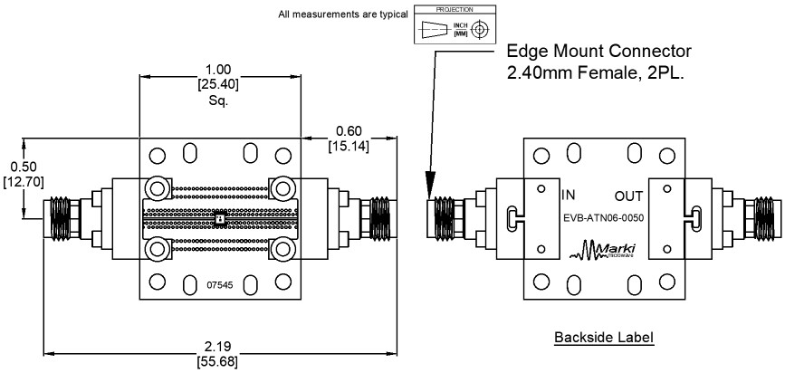
| EVB-ATN06-0050 | Evaluation Board, Chip Scale Package MMIC 50 GHz 6dB Attenuator | EVB | REACH RoHS | Released | EAR99 | - |
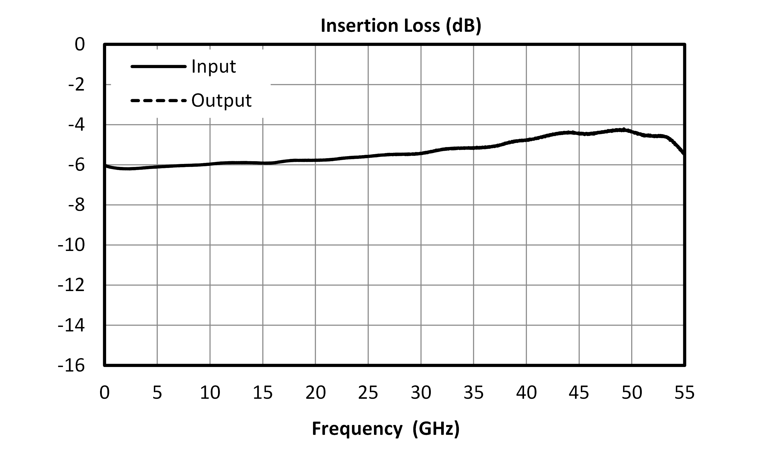
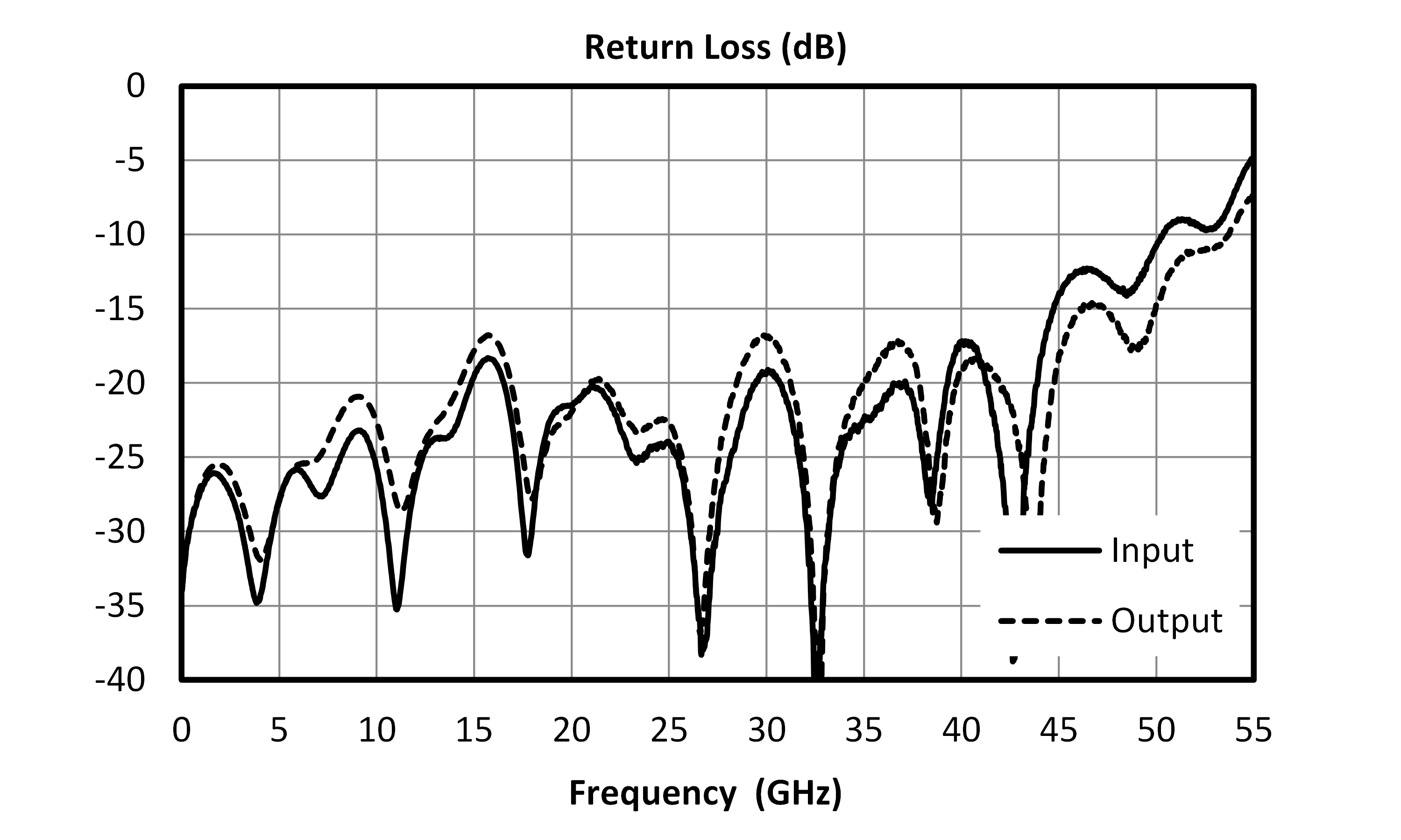
Electrical Performance Data is de-embedded to the CSP package ports.
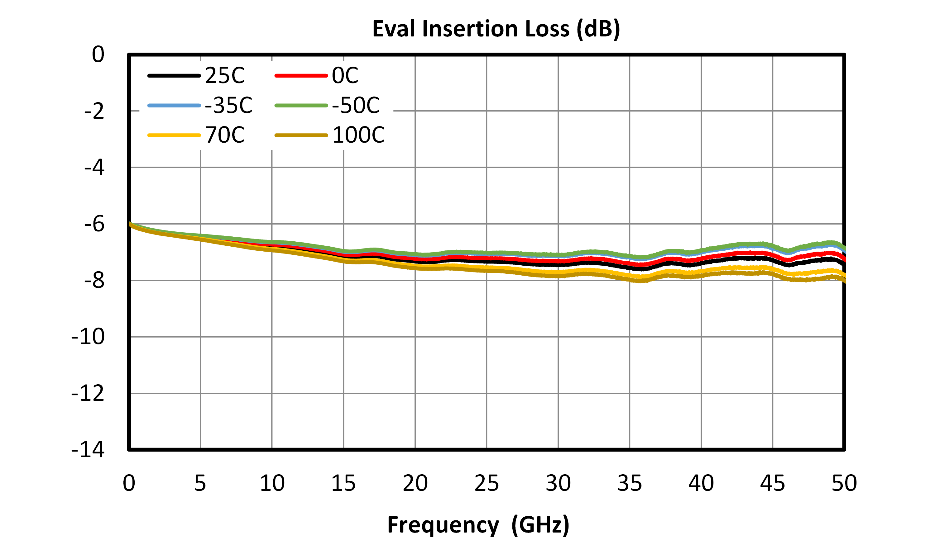
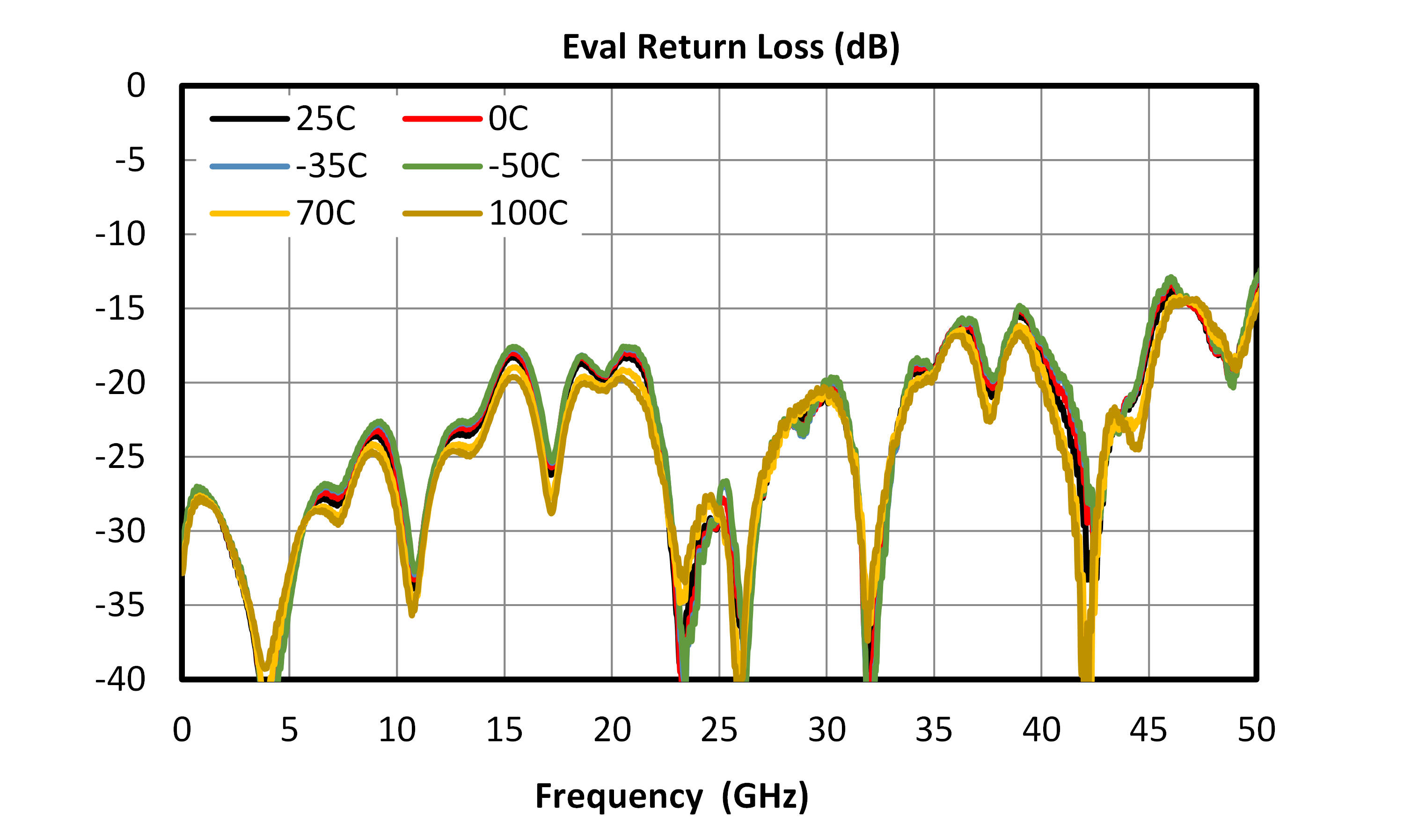
Evaluation board performance is shown as a proxy for device performance due to fixturing variability over temperature
The electrical specifications apply at TA=+25°C in a 50Ω system. Typical data shown is for the attenuator in a CSP package with a sine wave input applied to port 1.
| Parameter | Port Configuration | Test Conditions | Minimum Frequency (GHz) | Maximum Frequency (GHz) | Min | Typ | Max | Unit |
|---|---|---|---|---|---|---|---|---|
| Frequency Range | - | - | 0 | 50 | - | - | - | GHz |
| Attenuation | - | - | 30 | 50 | - | 4.75 | - | dB |
| Attenuation | - | - | 0 | 30 | - | 5.9 | - | dB |
| Impedance | - | - | 0 | 50 | - | 50 | - | Ω |
| Return Loss | - | - | 0 | 40 | 13 | 20 | - | dB |
| Return Loss | - | - | 40 | 50 | - | 14 | - | dB |
The Absolute Maximum Ratings indicate limits beyond which damage may occur to the device. If these limits are exceeded, the device may be inoperable or have a reduced lifetime.
| Parameter | Maximum Rating | Unit |
|---|---|---|
| Maximum Operating Temperature | 100 | °C |
| Maximum Storage Temperature | 125 | °C |
| Minimum Operating Temperature | -55 | °C |
| Minimum Storage Temperature | -65 | °C |
| RF Power Handling | 1 | W |
| Parameter | Details | Rating |
|---|---|---|
| ESD | 250 to < 500 Volts | HBM Class 1A |
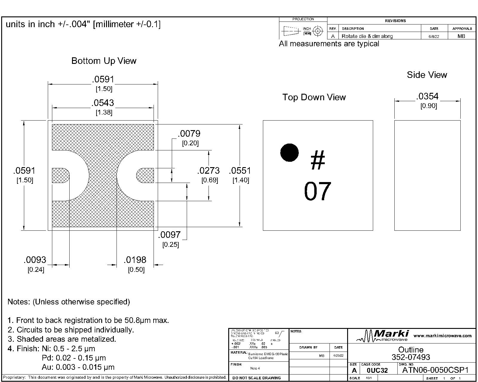
| Dimensions | - | 1.5 x 1.5 mm |
| Moisture Sensitivity Level | - | MSL 3 |

| Port | Function | Description | DC Equivalent Circuit |
|---|---|---|---|
| Ground Paddle | Ground | CSP package ground path is provided through the ground paddle. |  |
| Pin 1 | Input/Output | Pin 1 and Pin 2 are DC connected to each other and ground through a T-network of resistors. |  |
| Port | Function | Description | DC Equivalent Circuit |
|---|---|---|---|
| Ground Paddle | Ground | CSP1 package ground path is provided through the ground paddle. | |
| Pin 1 | Input/Output | Pin 1 and Pin 2 are DC connected to each other and ground through a T-network of resistors. | |
| Pin 2 | Input/Output | Pin 1 and Pin 2 are DC connected to each other and ground through a T-network of resistors. | |
Download : Outline 2D Drawing Outline 3D Drawing Outline 3D STP
Download : Footprint Drawing

| Revision Code | Revision Date | Comment |
|---|---|---|
| - | 2022-08-11 | Initial Release |
| A | 2025-04-15 | NRND |
MARKI MICROWAVE, LLC., (“MARKI”) PROVIDES TECHNICAL SPECIFICATIONS AND DATA (INCLUDING DATASHEETS), APPLICATION OR OTHER DESIGN ADVICE, WEB TOOLS, AND OTHER INFORMATION AND RESOURCES “AS IS” AND WITH ALL FAULTS. MARKI DISCLAIMS ALL WARRANTIES, EXPRESS OR IMPLIED, INCLUDING, WITHOUT LIMITATION, ANY IMPLIED WARRANTIES OF MERCHANTABILITY, FITNESS FOR A PARTICULAR PURPOSE, OR NON-INFRINGEMENT.
These resources are intended for developers skilled in the art designing with Marki products. You are solely responsible for (1) selecting the appropriate products for your application, (2) designing, validating, and testing your application, and (3) ensuring your application meets applicable standards and other requirements. Marki makes no guarantee regarding the suitability of its products for any particular purpose, nor does Marki assume any liability whatsoever arising out of your use or application of any Marki product.
Marki grants you permission to use these resources only for development of an application that uses Marki products. Other reproduction or use of these resources is strictly prohibited. No license is granted to any other Marki intellectual property or to any third-party intellectual property. Marki reserves the right to make changes to the product(s) or information contained herein without notice.
MARKI MICROWAVE, M wave logo, FastSwitch, and T3 MIXER are trademarks or registered trademarks of Marki Microwave, LLC. All other trademarks used are the property of their respective owners.
© 2022, 2025, Marki Microwave, LLC