Device Overview

General Description

The ATD01-0040PSM is a surface mount GaAs MMIC 1dB differential attenuator housed in a DFN package. This attenuator is an ideal solution for attenuating differential signals and can be used in a wide range of applications. The compact DFN package allows for extreme miniaturization of SMT footprints. GaAs MMIC technology provides consistent unit-to-unit performance in a small, low-cost form factor. A 50-ohm match is maintained over the entire operating frequency range.

Photo of ATD01-0040PSM

Features

  • Small 1.3 x 2.0 mm Package Size
  • 1dB Attenuation From DC to 40 GHz
  • 23dB Typical Return Loss Over Operating Band

Applications

  • Test Equipment
  • Electronic Warfare
  • Radar and satellite communications
  • High Channel Count Systems

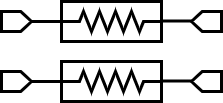
Functional Block Diagram

Block Diagram

Part Ordering Options

Part NumberDescriptionPackageGreen StatusProduct LifecycleExport Classification
ATD01-0040PSM1dB DC - 40GHz MMIC Differential AttenuatorDFN

REACH

RoHS

ReleasedEAR99
EVB-ATD01-0040PEvaluation Board, 1dB DC-40 GHz Differential AttenuatorEVB

REACH

RoHS

ReleasedEAR99

Table Of Contents

Revision History

Revision CodeRevision DateComment
-2026-05-26Initial Release

Rev: - | Copyright © 2026 Marki Microwave LLC.

2

Port Configuration and Functions

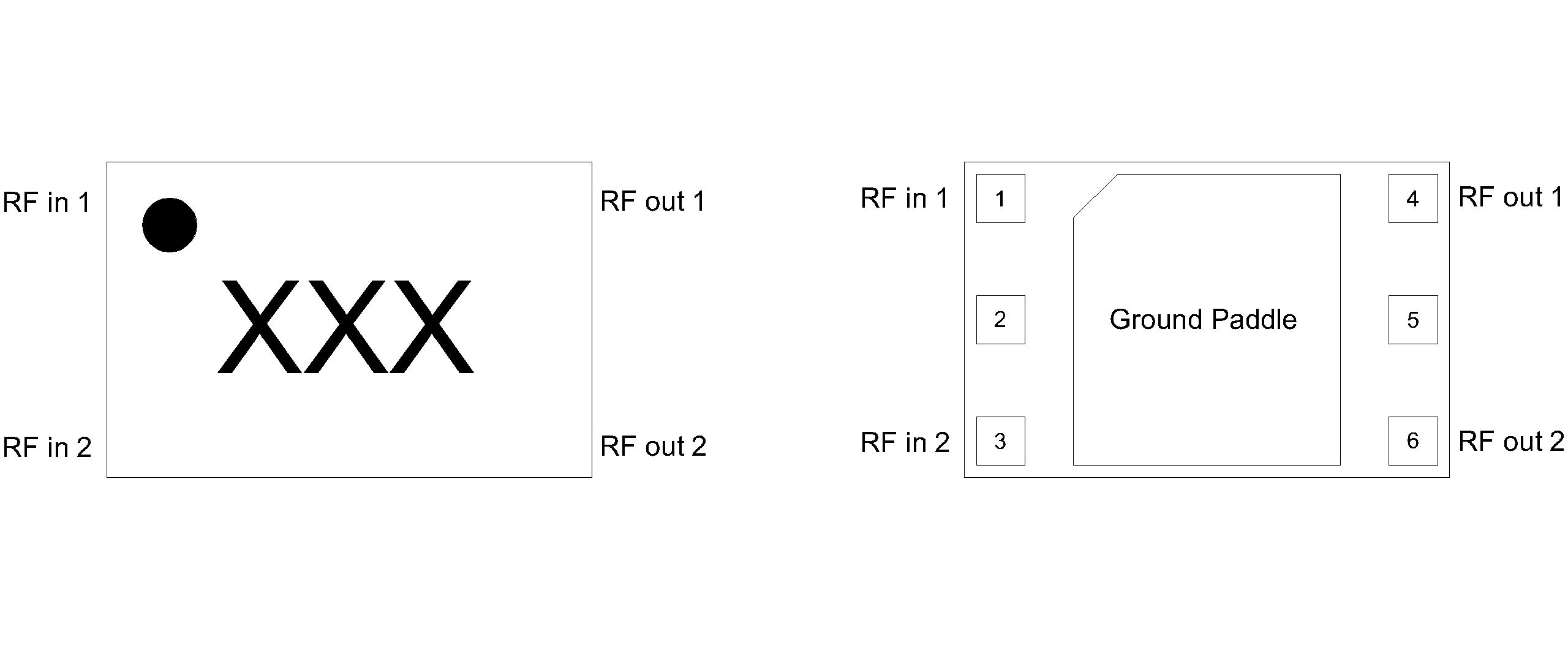
Port Diagram

Diagram of the port configuration for ATD01-0040PSM

Rev: - | Copyright © 2026 Marki Microwave LLC.

3

Port Functions

PortFunctionDescriptionDC Equivalent
Circuit
Ground PaddleGnd Ground paddle should be connected to RF groundEquivalent circuit for the Gnd
Pin 1Input/Output 1 Pin 1 and Pin 4 are DC connected to each other and ground through a T-network of resistors.Equivalent circuit for the Input/Output 1
Pin 2Non-connect (NC) Pin 2 is not connected internally and should be tied to RF ground.Equivalent circuit for the Non-connect (NC)
Pin 3Input/Output 2 Pin 3 and Pin 6 are DC connected to each other and ground through a T-network of resistors.Equivalent circuit for the Input/Output 2
Pin 4Input/Output 1 Pin 4 and Pin 1 are DC connected to each other and ground through a T-network of resistors.Equivalent circuit for the Input/Output 1
Pin 5Non-connect (NC) Pin 5 is not connected internally and should be tied to RF ground.Equivalent circuit for the Non-connect (NC)
Pin 6Input/Output 2 Pin 6 and Pin 3 are DC connected to each other and ground through a T-network of resistors.Equivalent circuit for the Input/Output 2

Rev: - | Copyright © 2026 Marki Microwave LLC.

4

Specifications

Absolute Maximum Ratings

The Absolute Maximum Ratings indicate limits beyond which damage may occur to the device. If these limits are exceeded, the device may be inoperable or have a reduced lifetime.

ParameterMaximum RatingUnit
Maximum Operating Temperature 100°C
Maximum Storage Temperature 125°C
Minimum Operating Temperature -55°C
Minimum Storage Temperature -65°C
DC Current 16mA
RF Power Handling 8W

Power handling tested with a continuous wave at 18GHz.

Package Information

ParameterDetailsRating
ESD250 to < 500 VoltsHBM Class 1A
Dimensions-2.0 x 1.3 mm
Moisture Sensitivity Level-MSL 1

Rev: - | Copyright © 2026 Marki Microwave LLC.

5

Electrical Specifications

The electrical specifications apply at TA=+25°C in a 50Ω system. Min and Max limits are guaranteed at TA=+25°C. Attenuation paths 1 and 2 are symmetrical and have the same typical performance.

ParameterTest ConditionsMinimum
Frequency
(GHz)
Maximum
Frequency
(GHz)
MinTypMaxUnit
Attenuation Temp = 25°C
0 40-1.3-dB
Return Loss Temp = 25°C
0 40-23-dB
Attenuation Flatness Temp = 25°C
0 40-0.7-dB
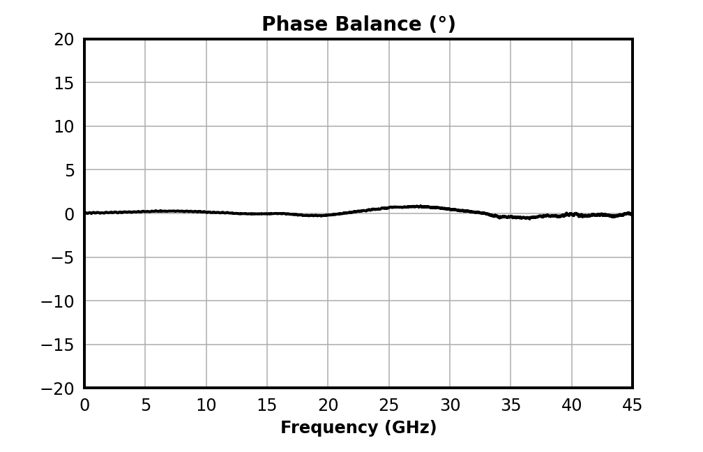
Phase Balance -0 40-0.3-°
Amplitude Balance -0 40-0-dB

Rev: - | Copyright © 2026 Marki Microwave LLC.

6

Typical Performance Plot

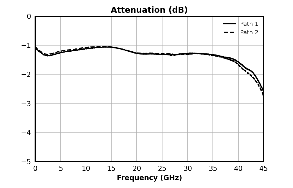
Attenuation (dB) graph for ATD01-0040PSM
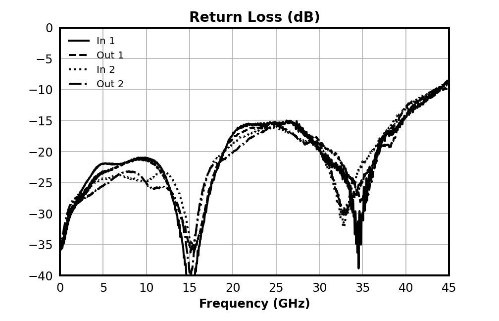
Return Loss (dB) graph for ATD01-0040PSM
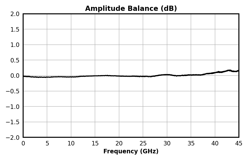
Amplitude Balance (dB) graph for ATD01-0040PSM
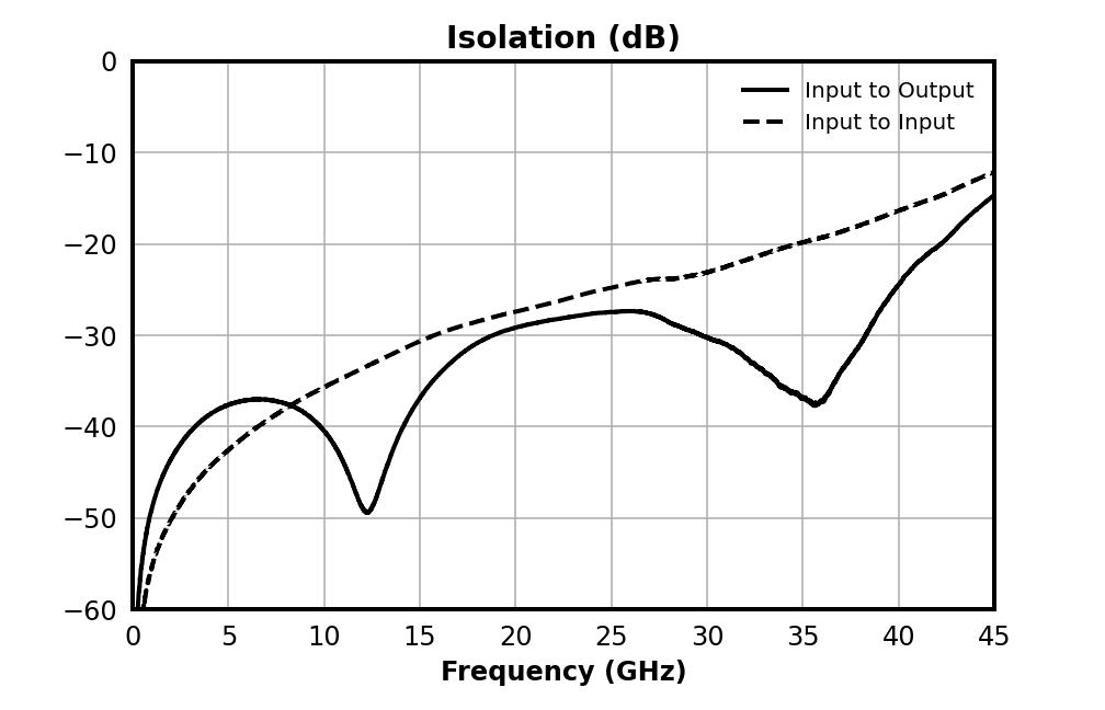
Path 1 to Path 2 Isolation graph for ATD01-0040PSM
Phase Balance (°) graph for ATD01-0040PSM

Rev: - | Copyright © 2026 Marki Microwave LLC.

7

Typical Mixed Mode Performance Plots

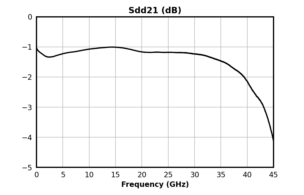
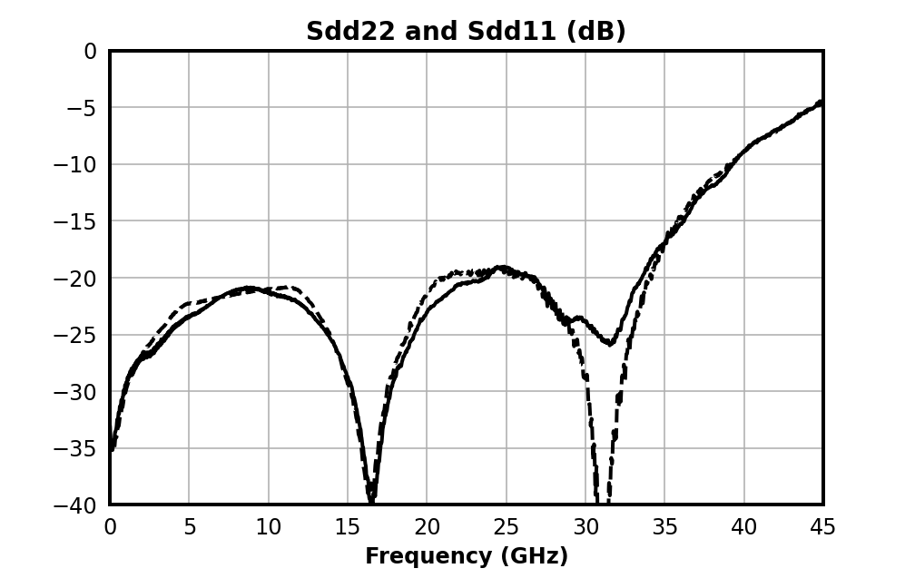
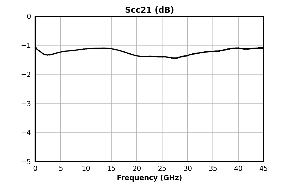
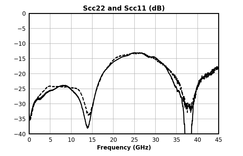
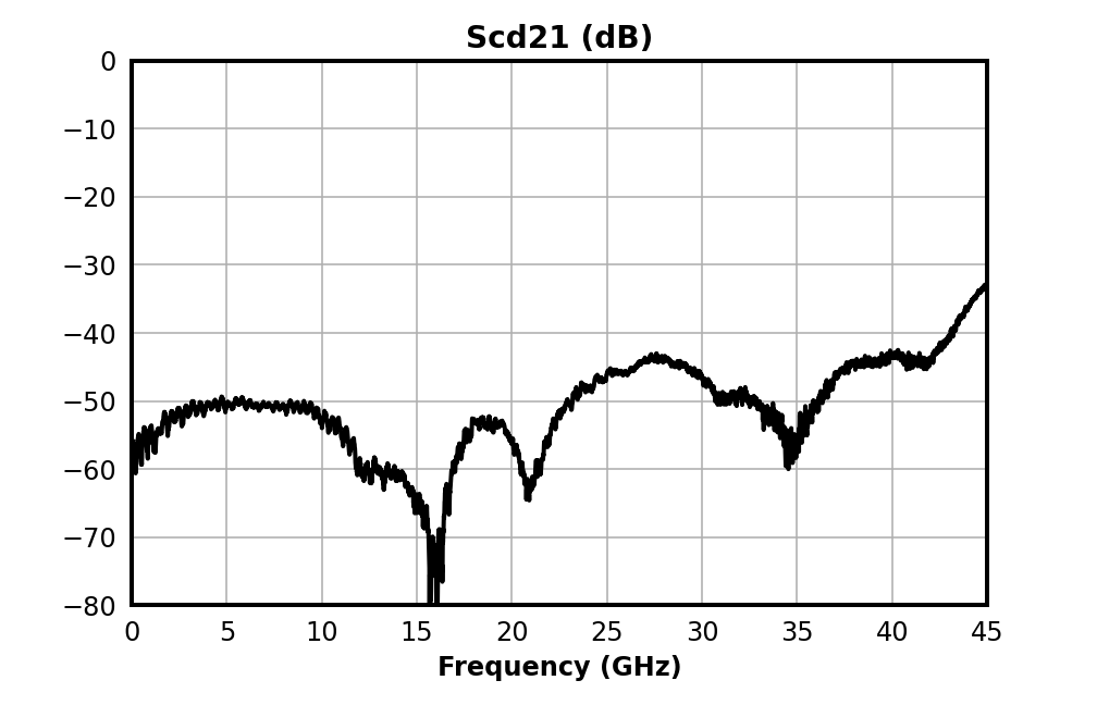
Mixed mode scattering parameters are used to characterize differential circuits. For differential attenuators this means that the 2 input ports become a single 100Ω differential port and the 2 output ports become a single 100Ω differential port. The two-port s-parameters of the differential attenuators are then characterized based on differential (d) signals.

Insertion Loss of a Differential Signal graph for ATD01-0040PSM
Return loss of a differential signal (dB) graph for ATD01-0040PSM
Common Mode Insertion Loss (dB) graph for ATD01-0040PSM
Common Mode Return Loss (dB) graph for ATD01-0040PSM
Common Mode Insertion Loss given a Differential Input (dB) graph for ATD01-0040PSM

Measured data is de-embedded from fixture using AFR.

Rev: - | Copyright © 2026 Marki Microwave LLC.

8

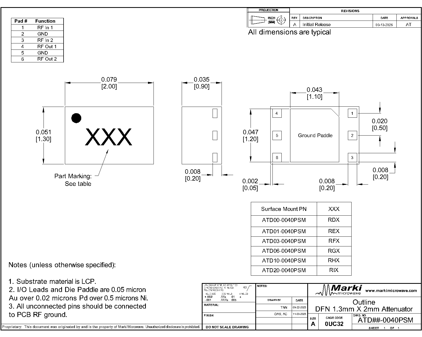
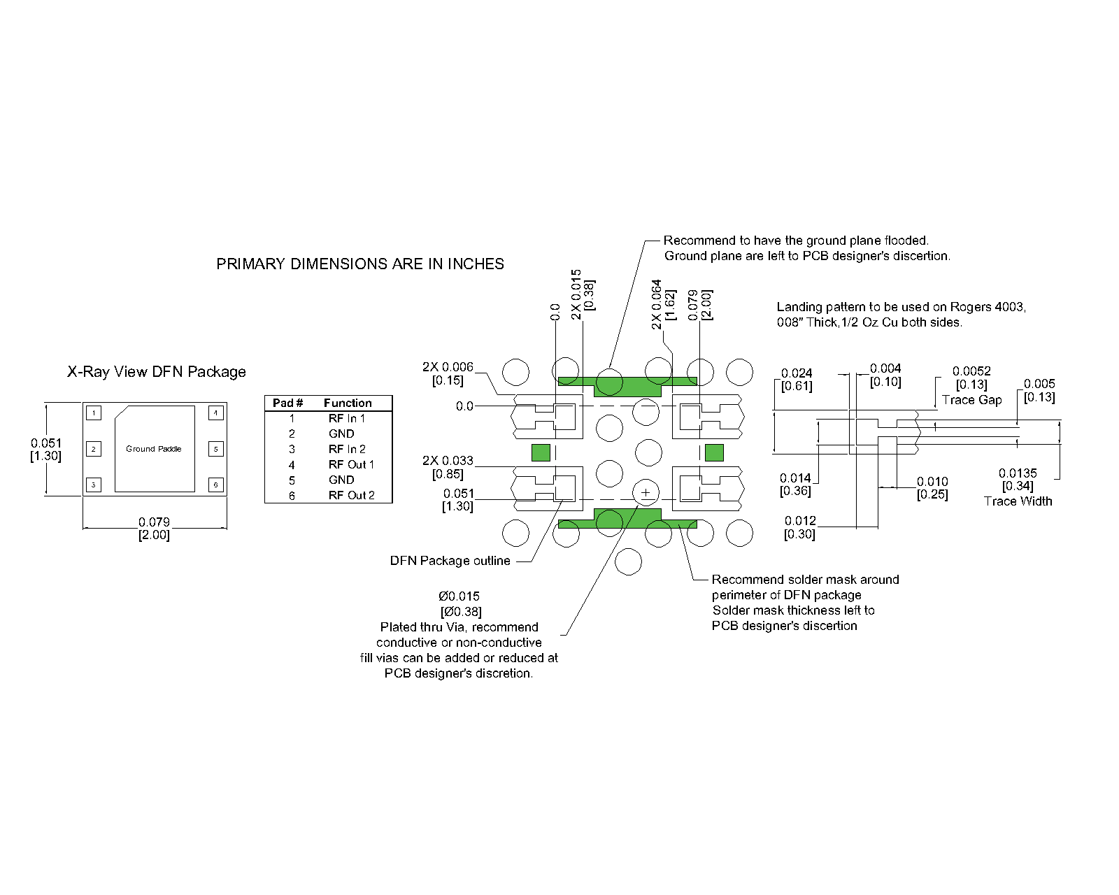
Mechanical Data

Rev: - | Copyright © 2026 Marki Microwave LLC.

9

Rev: - | Copyright © 2026 Marki Microwave LLC.

10

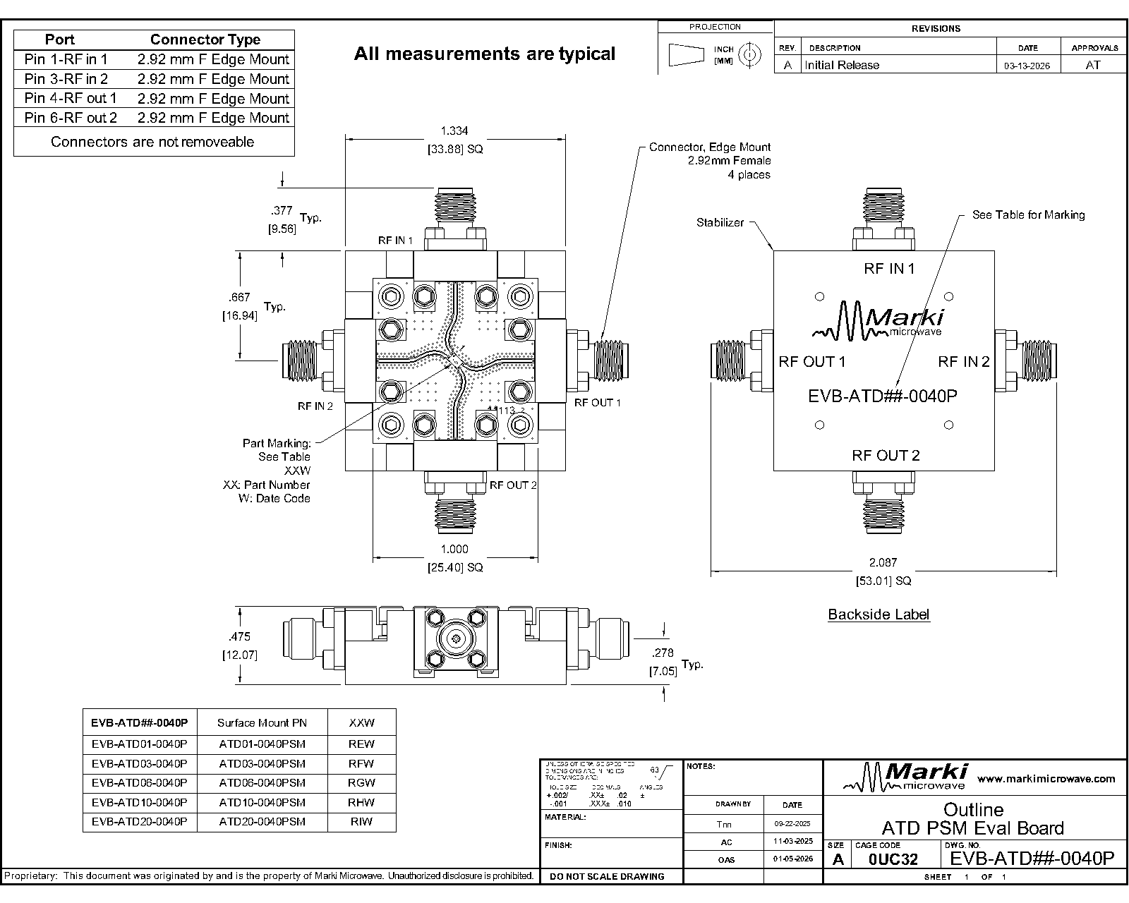
Evaluation Board - Outline Drawing

Outline Drawing

Rev: - | Copyright © 2026 Marki Microwave LLC.

11