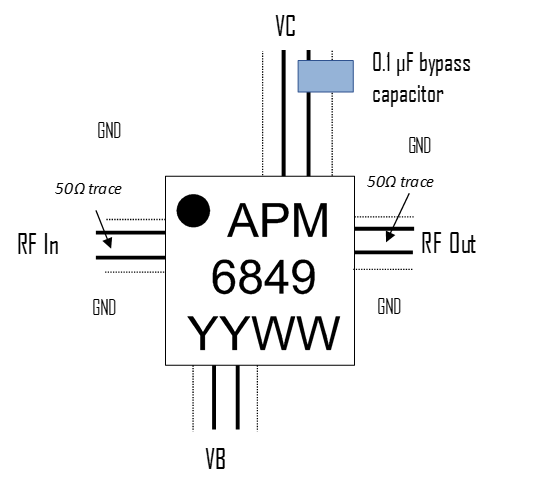
Port Diagram
Sales: 408-778-9952 | General: 408-778-4200 | Fax: 408-778-4300
Sales & Customer Support: [email protected]
Tech Support: [email protected]
The APM-6849SM is a single stage broadband, low phase noise pre-amplifier designed to provide 11 dB typical gain packaged in a 3 mm QFN with low current consumption. This amplifier uses GaAs HBT technology for low phase noise, and provides industry leading 170 dBc/Hz at 10 kHz offset from carrier frequency. It offers low power dissipation while providing sufficient gain and power to drive a saturated LO driver amplifier such as the APM-7516SM, APM-7098SM, or APM-7099SM.

| Part Number | Description | Package | Packing Size | Green Status | Product Lifecycle | Export Classification |
|---|---|---|---|---|---|---|
| APM-6849SM | 2-30 GHz Surface Mount Low Phase Noise Amplifier | QFN | - | REACH RoHS | Released | EAR99 |
| EVAL-APM-6849SM | Evaluation Board, Low Phase Noise 2 – 30 GHz Amplifier | EVAL | - | REACH RoHS | Released | EAR99 |
| APM-6849-TR | Tape and Reel, 2-30 GHz Surface Mount Low Phase Noise Amplifier | QFN | 7" | REACH RoHS | Released | EAR99 |
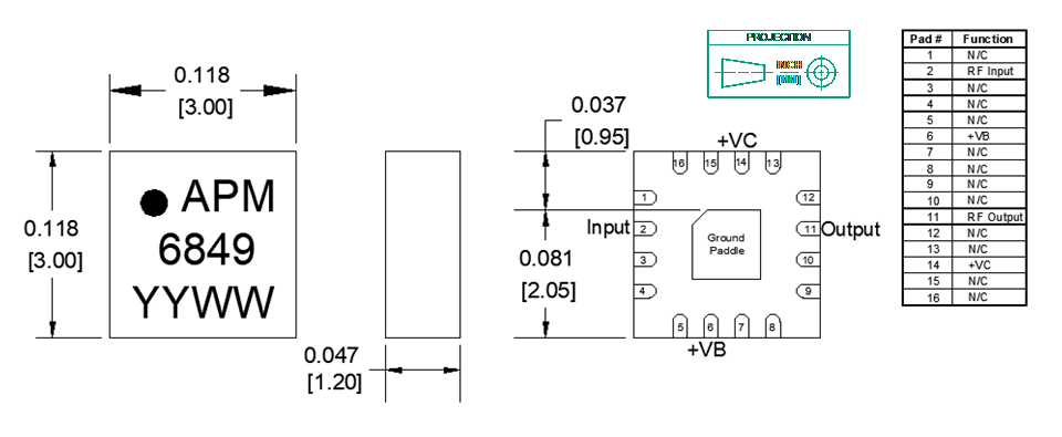
APM-6849SM
2-30 GHz Surface Mount Low Phase Noise Amplifier
| Revision Code | Revision Date | Comment |
|---|---|---|
| - | 2019-11-01 | Datasheet Initial Release |
| A | 2020-05-01 | Updated EVAL board outline |
| B | 2020-07-01 | Updated Small Signal Gain Min Spec |
| C | 2020-07-01 | Updated Max Operating Temperature |
| D | 2020-10-01 | Updated Min Specs and Input Power for Saturation |
| E | 2020-11-01 | Updated Thermal Specs and Min Specs, added link |
| F | 2022-01-01 | Updated device description, input power limit, and plots |
APM-6849SM
2-30 GHz Surface Mount Low Phase Noise Amplifier
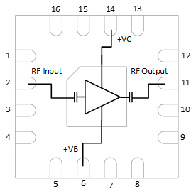
| Port | Function | Description | DC Equivalent Circuit |
|---|---|---|---|
| 11 | RF Output | Pin 11 is the amplifier die RF Output port. It is internally DC blocked and RF matched to 50 Ω. Must have less than 7:1 VSWR when operating with voltage greater than 5V on VC. |  |
| 14 | Collector Supply Port | Pin 14 is the amplifier IC’s DC voltage supply pad. See section 3.6 for performance at different bias conditions. |  |
| 2 | RF Input | This is the amplifier die RF Input port. It is internally DC blocked and RF matched to 50 Ω. | |
| 6 | Base Supply Port | Pin 6 is the current mirror DC voltage supply port that controls the collector current supplied to the amplifier. VB port voltage is proportional to VC port collector current. VB effectively functions as a gain control pin. See section 3.6 for performance at different bias conditions. |  |
| GND | Ground | Pin 11 is the amplifier die RF Output port. It is internally DC blocked and RF matched to 50 Ω. Must have less than 7:1 VSWR when operating with voltage greater than 5V on VC. |  |
APM-6849SM
2-30 GHz Surface Mount Low Phase Noise Amplifier
The Absolute Maximum Ratings indicate limits beyond which damage may occur to the device. If these limits are exceeded, the device may become inoperable or have a reduced lifetime.
| Parameter | Maximum Rating | Unit |
|---|---|---|
| Collector Positive Bias Voltage (Vc) | 7 | V |
| Current Mirror Positive Bias Current (Ib) | 4 | mA |
| Current Mirror Positive Bias Voltage (VB) | 7 | V |
| Maximum Operating Temperature | 85 | °C |
| Maximum Storage Temperature | 150 | °C |
| Max Junction Temperature for MTTF > 1E6 Hours | 125 | °C |
| Minimum Operating Temperature | -40 | °C |
| Minimum Storage Temperature | -65 | °C |
| Output Load VSWR | 7 | - |
| Positive Bias Current (Ic) | 90 | mA |
| RF Input Power 1 | 16 | dBm |
| θJC | 78 | ºC/W |
[1] Maximum RF input power for instantaneous failure. Reliable operation requires RF input power limited to maintain Positive Bias Current Ic within reliable limits.
| Parameter | Details | Rating |
|---|---|---|
| Dimensions | - | 3 x 3 mm |
| Moisture Sensitivity Level | - | MSL 1 |
The Recommended Operating Conditions indicate the limits, inside which the device should be operated, to guarantee the performance given in Electrical Specifications Operating outside these limits may not necessarily cause damage to the device, but the performance may degrade outside the limits of the electrical specifications. For limits, above which damage may occur, see Absolute Maximum Ratings.
| Parameter | Min | Nominal | Max | Unit |
|---|---|---|---|---|
| Ambient Temperature | -40 | 25 | 85 | °C |
| Positive DC Voltage (VC) | 3 | 5 | 6 | V |
| Positive DC Current (Ic) | 8 | 21 | 32 | mA |
| Positive DC Current Mirror Voltage (VB) | 3 | 5 | 6 | V |
| Positive DC Current Mirror Current (Ib) | 0.9 | 2 | 2.6 | mA |
APM-6849SM
2-30 GHz Surface Mount Low Phase Noise Amplifier
The electrical specifications apply at TA=+25°C in a 50Ω system. QFNs are 100% RF tested.
| Parameter | Test Conditions | Minimum Frequency (GHz) | Maximum Frequency (GHz) | Min | Typ | Max | Unit |
|---|---|---|---|---|---|---|---|
| Current Consumption 1 | 5V/4V | - | - | - | 13 | - | mA |
| Current Consumption 2 | 5V/5V | - | - | - | 21 | - | mA |
| Current Consumption 3 | 5V/6V | - | - | - | 32 | - | mA |
| Input IP3 | 5V/5V bias, -15 dBm Input Power | 2 | 30 | - | 11 | - | dBm |
| Input Return Loss | 5V/5V bias, -25 dBm Input Power | 2 | 20 | - | 15 | - | dB |
| Input Return Loss | 5V/5V bias, -25 dBm Input Power | 20 | 30 | - | 15 | - | dB |
| Noise Figure | 5V/5V bias, -25 dBm Input Power | 2 | 26.5 | - | 5 | - | dB |
| Output IP3 | 5V/5V bias, -15 dBm Input Power | 2 | 30 | - | 20 | - | dBm |
| Output P1dB | 5V/5V bias | 20 | 30 | - | 14 | - | dBm |
| Output P1dB | 5V/5V bias | 2 | 20 | - | 20 | - | dBm |
| Output Return Loss | 5V/5V bias, -25 dBm Input Power | 20 | 30 | - | 8 | - | dB |
| Output Return Loss | 5V/5V bias, -25 dBm Input Power | 2 | 20 | - | 16 | - | dB |
| Phase Noise @ 10 kHz Offset | 5V/5V bias, +9 dBm Input power | 2 | 30 | - | -170 | - | dBc/Hz |
| Reverse Isolation | 5V/5V bias, -25 dBm Input Power | 2 | 30 | - | 42 | - | dB |
| Saturated Output Power | 5V/5V bias, Ic=90mA | 2 | 20 | - | 21 | - | dBm |
| Small Signal Gain | 5V/5V bias, -25 dBm Input Power | 20 | 30 | - | 7.5 | - | dB |
| Small Signal Gain | 5V/5V bias, -25 dBm Input Power | 2 | 20 | 8 | 11 | - | dB |
[1][2][3] Bias conditions for Ic and Ib tested with no RF input power. See performance plots for DC current vs. RF power. Bias conditions presented as VC/VB.
APM-6849SM
2-30 GHz Surface Mount Low Phase Noise Amplifier
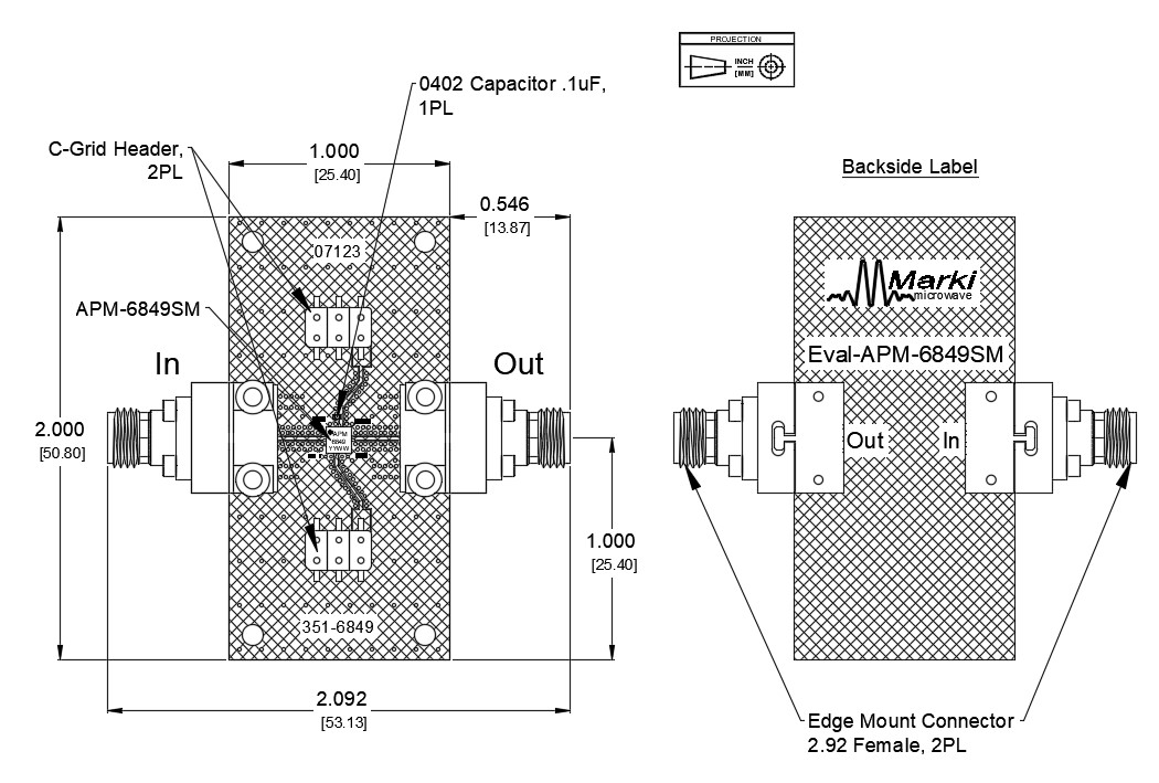
APM-6849SM measurements taken in EVAL-APM-6849 evaluation board.


APM-6849SM
2-30 GHz Surface Mount Low Phase Noise Amplifier


APM-6849SM
2-30 GHz Surface Mount Low Phase Noise Amplifier
Surface mount module APM-6849SM performance is expected to be similar to connectorized module performance.


APM-6849SM
2-30 GHz Surface Mount Low Phase Noise Amplifier
Fast rise time is desirable for linear T3 mixer operation. ( 5GHz on the left and 10GHz on the right )


APM-6849SM
2-30 GHz Surface Mount Low Phase Noise Amplifier
APM-6849SM
2-30 GHz Surface Mount Low Phase Noise Amplifier
APM-6849SM
2-30 GHz Surface Mount Low Phase Noise Amplifier
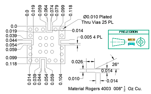
Download : Footprint Drawing
APM-6849SM
2-30 GHz Surface Mount Low Phase Noise Amplifier