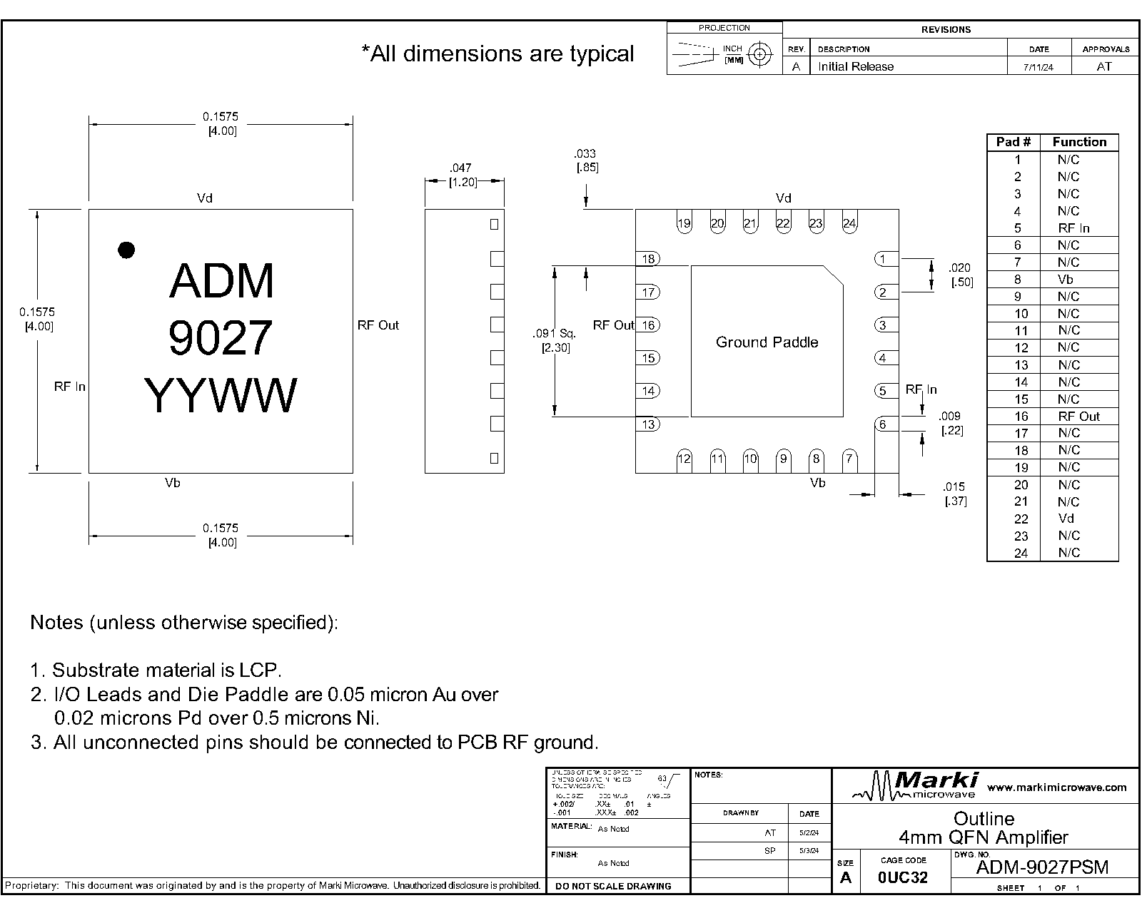
Absolute Maximum Ratings
The Absolute Maximum Ratings indicate limits beyond which damage may occur to the device. If any one of these limits are exceeded, the device may become inoperable or have a reduced lifetime. Reliability limits are individual, instantaneous catastrophic limits only. Functional operation limits are indicated below. Operation of the device at multiple absolute maximum limits or for extended periods at a single limit can cause degradation and damage to the device.
| Parameter | Maximum Rating | Unit |
|---|---|---|
| Bias Supply Voltage (Vb) | 6.5 | V |
| Drain Current (Id) (No RF Applied) | 85 | mA |
| Maximum Operating Temperature for MTTF > 1E6 hours | 85 | °C |
| Maximum Storage Temperature | 125 | °C |
| Minimum Operating Temperature for MTTF > 1E6 hours | -40 | °C |
| Minimum Storage Temperature | -65 | °C |
| Positive Drain Supply Voltage (Vd) | 8 | V |
| RF Input Power | 15 | dBm |
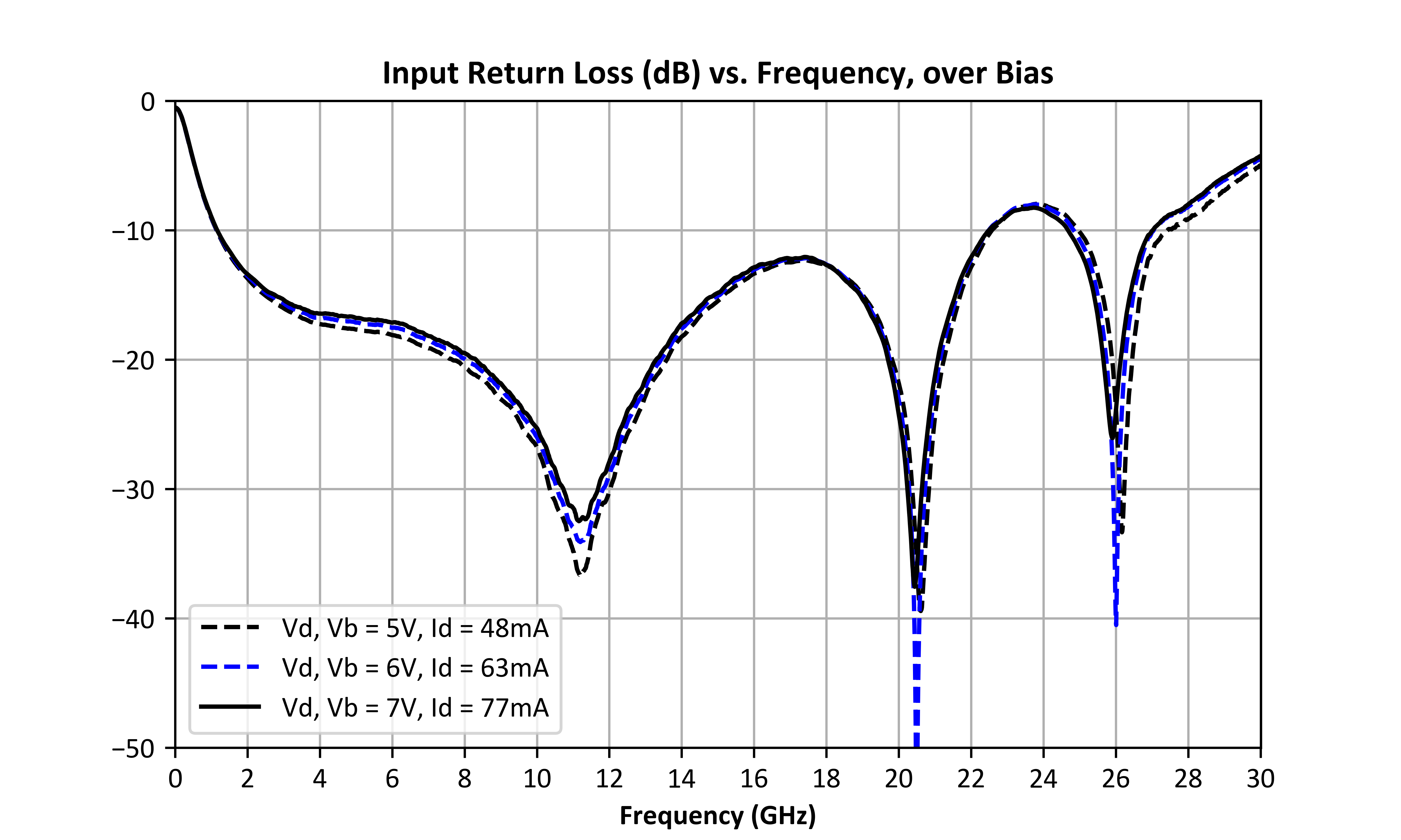
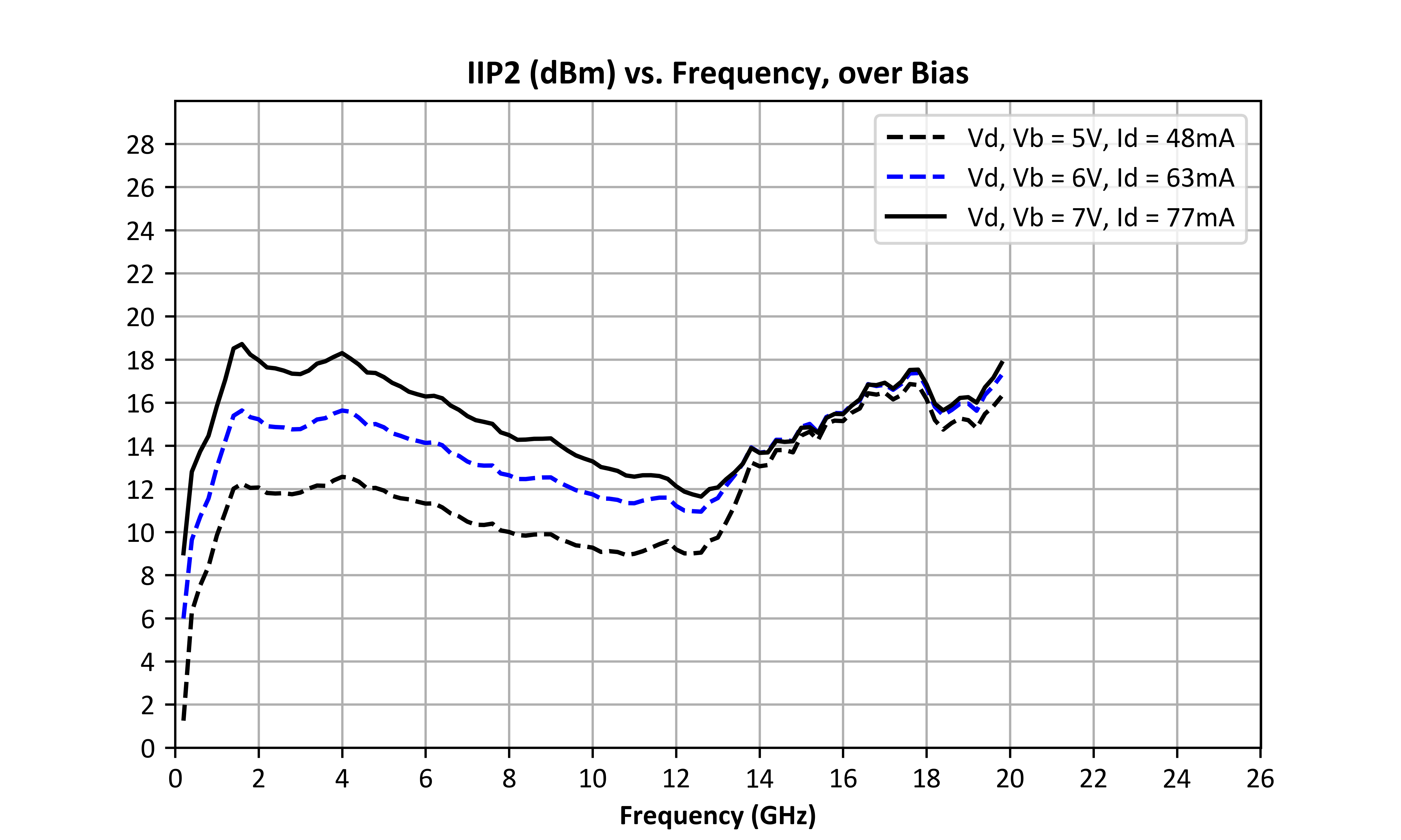
%20vs.%20Frequency,%20over%20Bias.png)
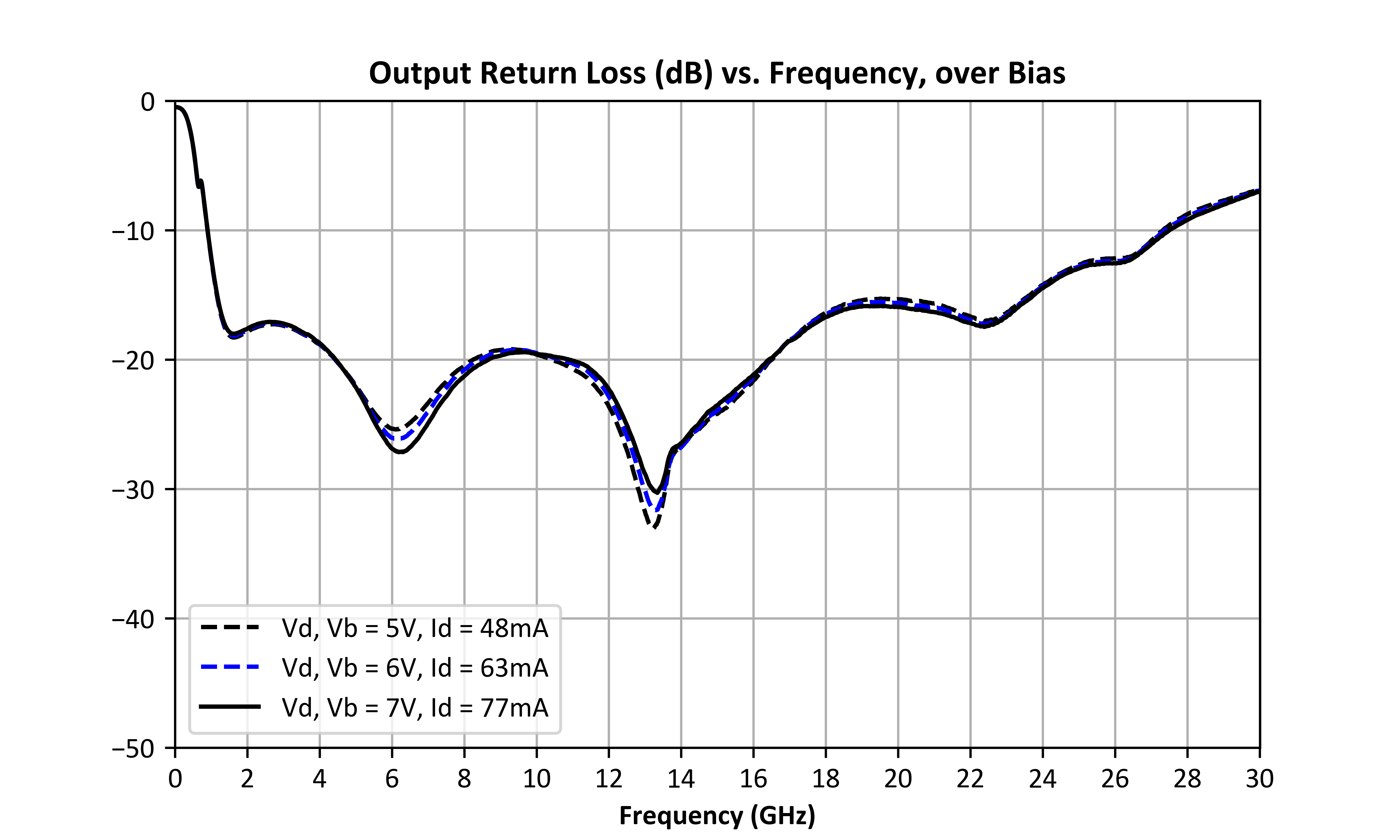
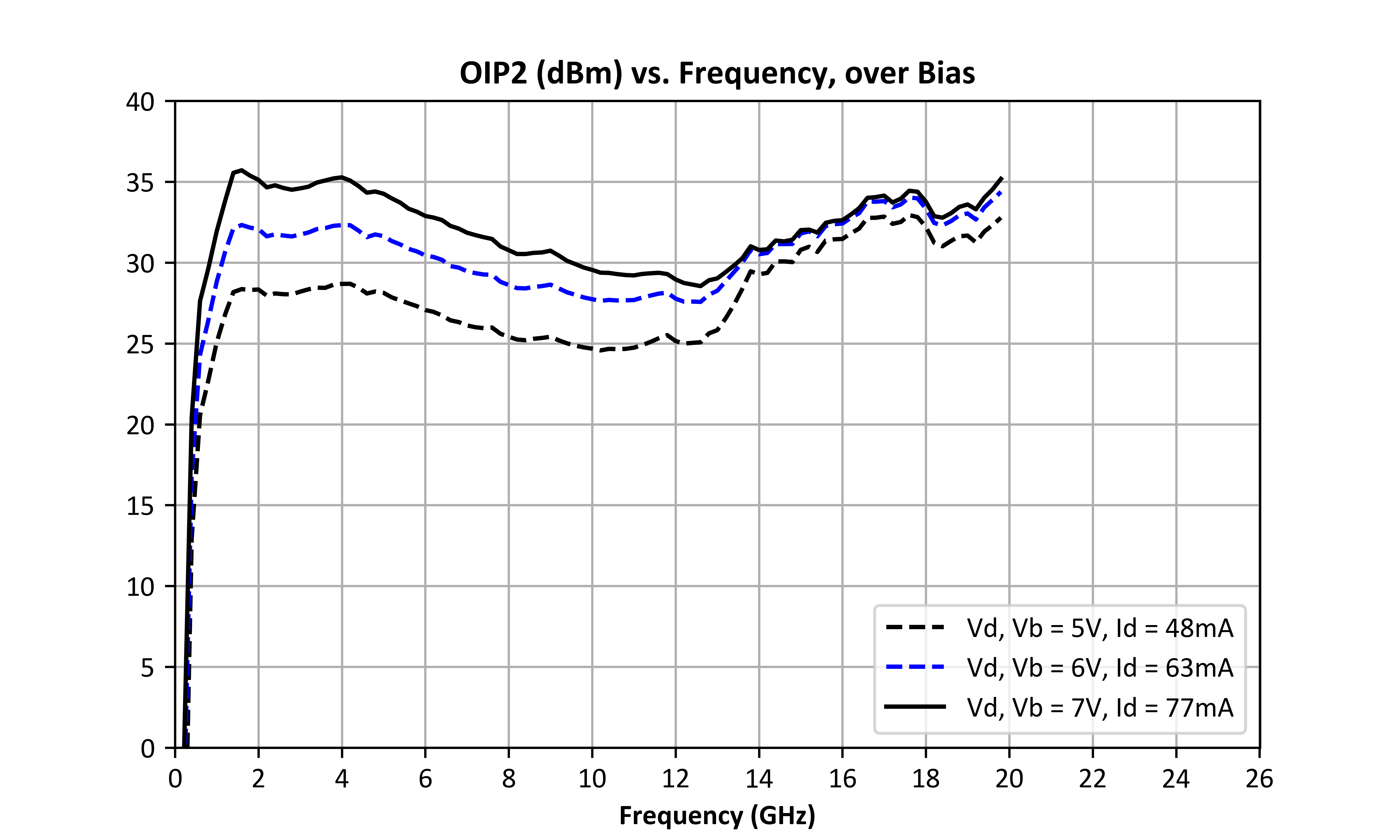
%20vs.%20Frequency,%20over%20Bias.png)
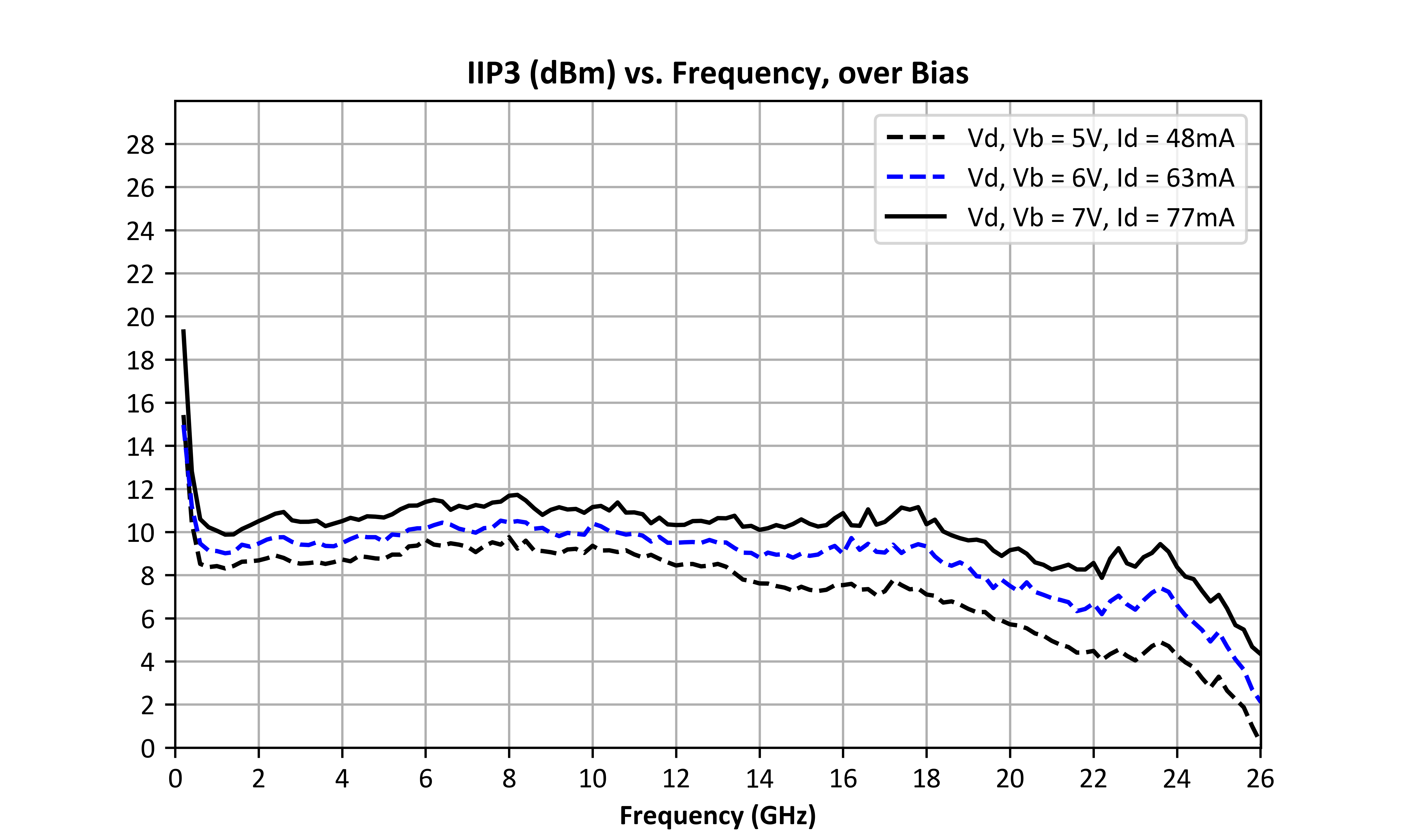
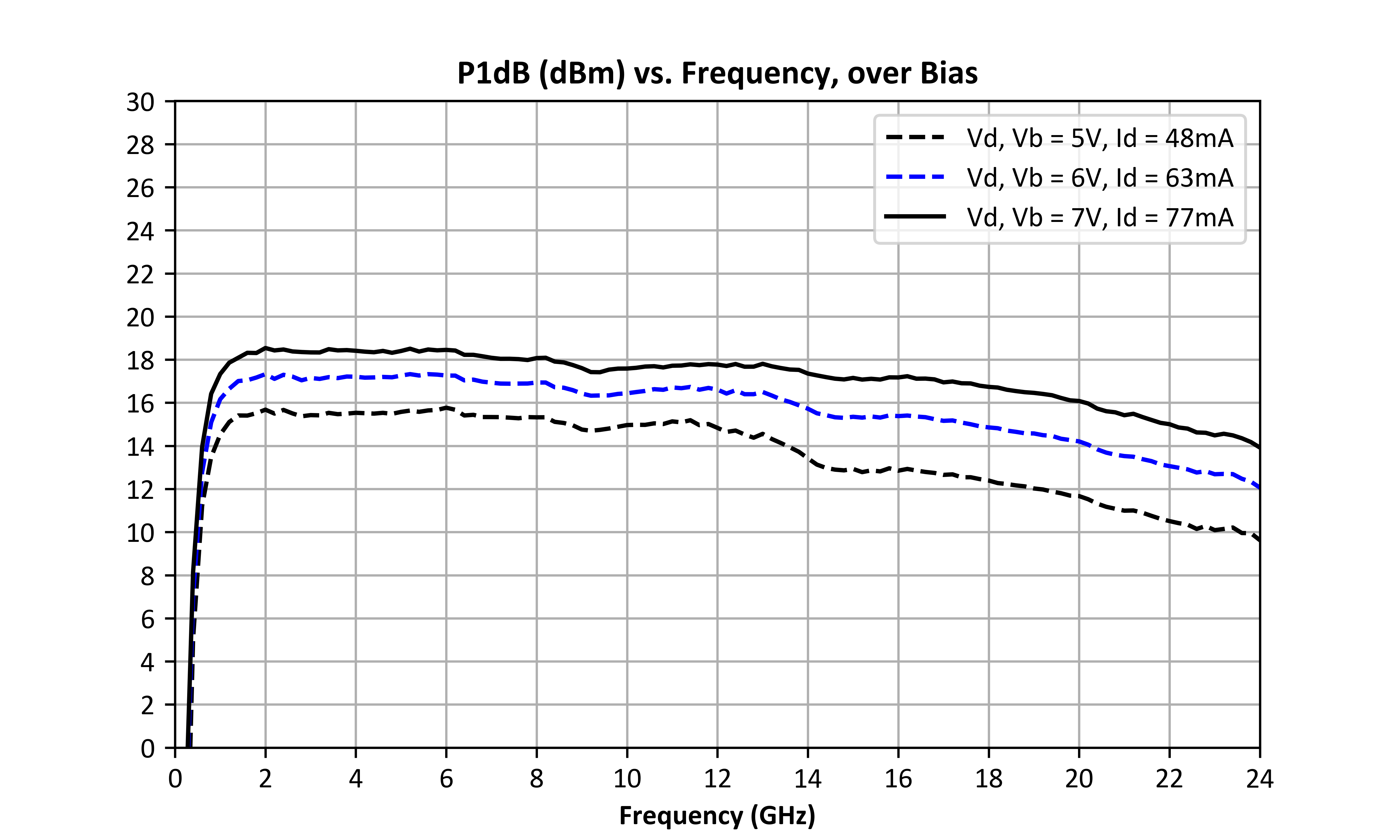
%20vs.%20Frequency,%20over%20Bias.png)
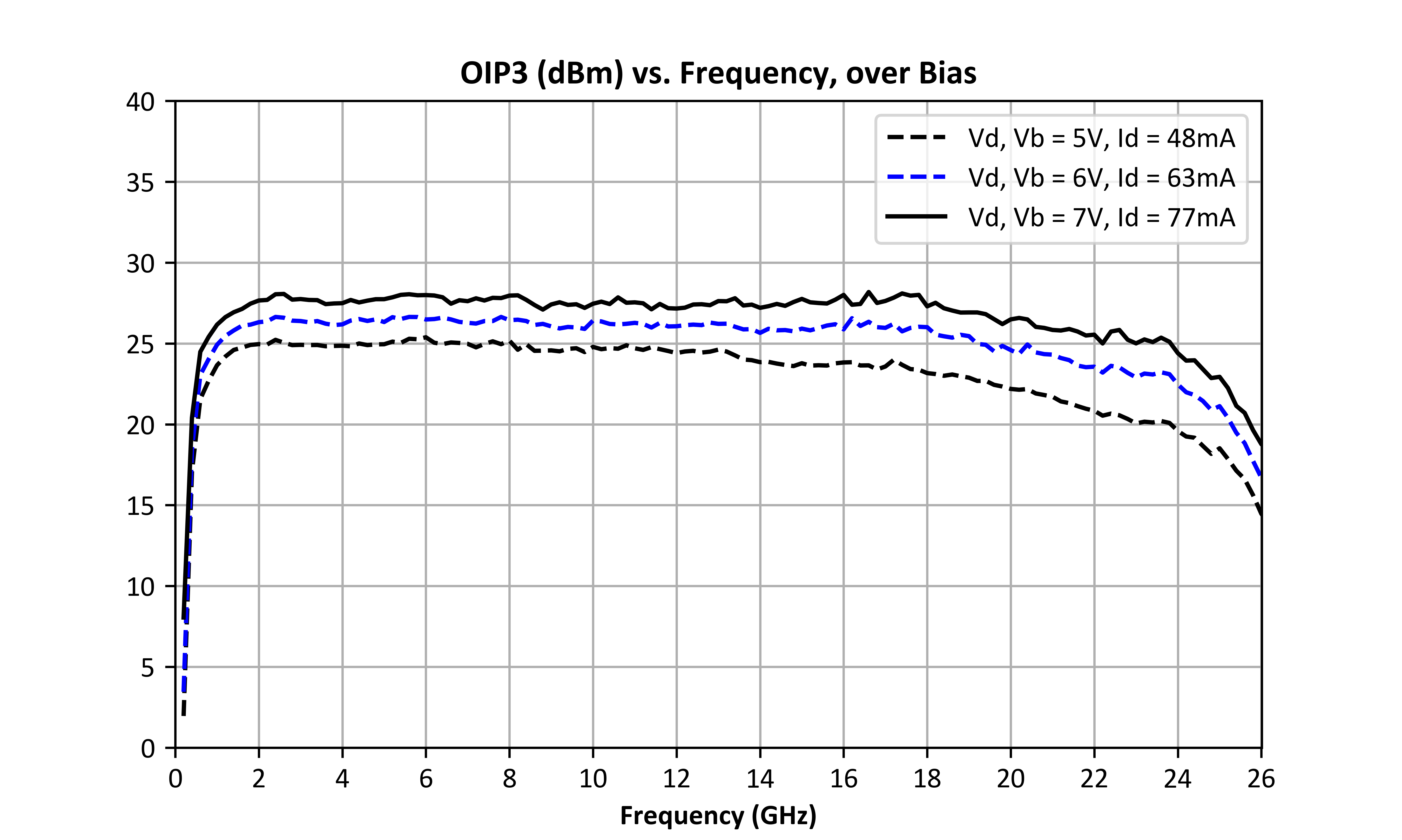
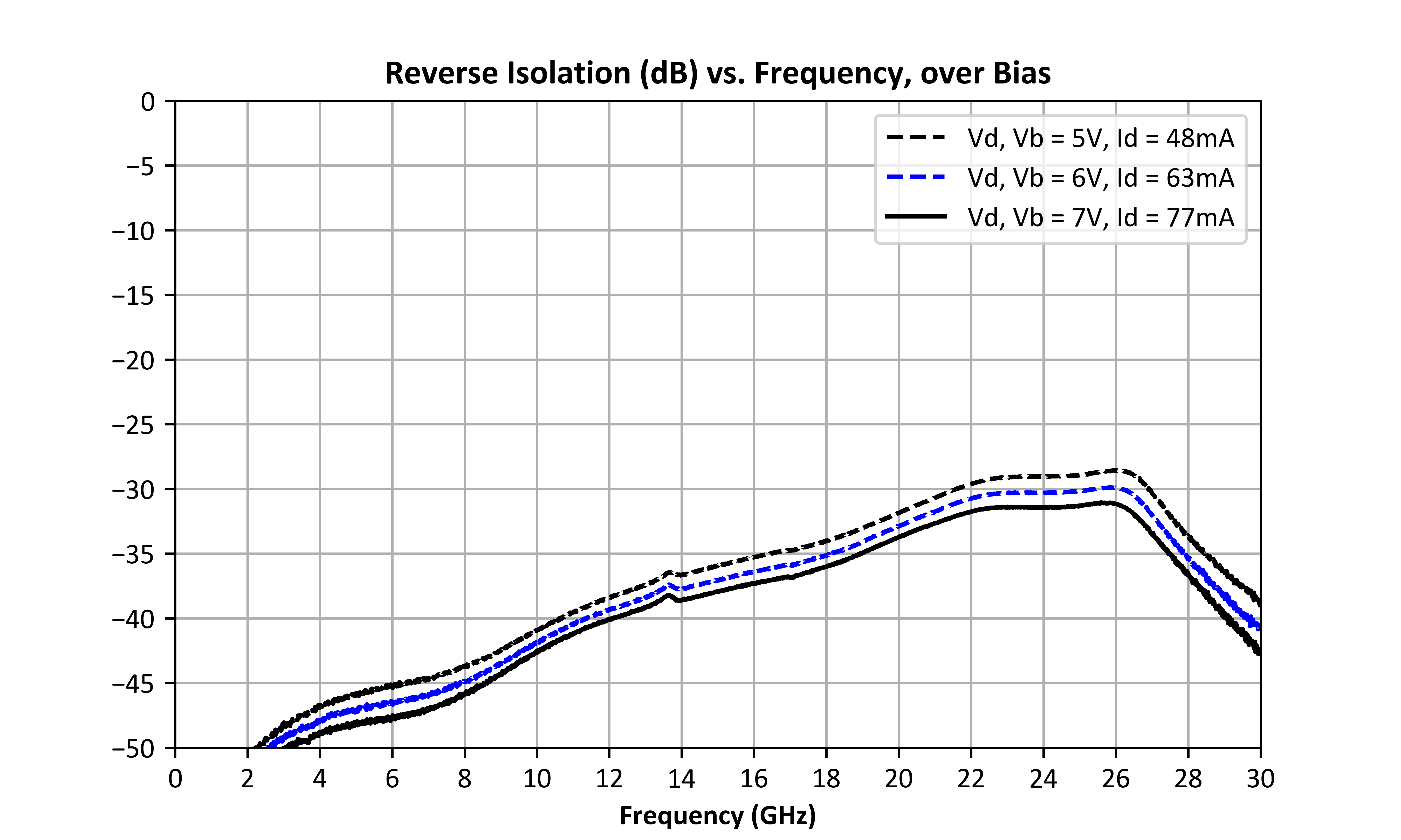
%20vs.%20Frequency,%20over%20Bias.png)
%20vs.%20Frequency,%20over%20Bias.png)
%20vs.%20Frequency,%20over%20Bias.png)
%20vs.%20Frequency,%20over%20Bias.png)
%20vs.%20Frequency,%20over%20Bias.png)
%20vs.%20Frequency,%20over%20Bias.png)
%20vs.%20Frequency,%20over%20Bias.png)