Port Diagram
Below is the port diagram from the ADM-8344PSM. The diagram is an x-ray view from the top down.

Sales: 408-778-9952 | General: 408-778-4200 | Fax: 408-778-4300
Sales & Customer Support: [email protected]
Tech Support: [email protected]
The ADM-8344PSM is a wideband distributed low noise amplifier capable of providing 19 dB gain and +29 dBm OIP3 from DC to 18 GHz and a low 1.7 dB typical noise figure from 4 to 14 GHz. The ADM-8344PSM is an ideal linear signal amplifier for applications requiring low power consumption and small form-factors. ADM-8344 is available A 4mm QFN and can be supplied from a single positive bias. The amplifier has excellent return losses and noise figure performance.

| Part Number | Description | Package | Green Status | Product Lifecycle | Export Classification |
|---|---|---|---|---|---|
| ADM-8344PSM | DC - 18 GHz Distributed Amplifier | PSM | RoHS REACH | Released | EAR99 |
| EVB-ADM-8344P | Evaluation Board, DC - 18 GHz Distributed Amplifier | EVB | REACH RoHS | Released | - |
ADM-8344PSM
DC - 18 GHz Distributed Amplifier
| Revision Code | Revision Date | Comment |
|---|---|---|
| - | 2025-06-13 | Initial Release |
ADM-8344PSM
DC - 18 GHz Distributed Amplifier
Below is the port diagram from the ADM-8344PSM. The diagram is an x-ray view from the top down.
ADM-8344PSM
DC - 18 GHz Distributed Amplifier
| Port | Function | Description | DC Equivalent Circuit |
|---|---|---|---|
| Paddle | Ground | The package ground paddle must be connected to a DC/RF ground potential with high thermal and electrical conductivity. |  |
| Pin 11 | ACG | This pin provides AC ground for the internal circuit. This pin should be connected to ground through a bypass capacitor as shown in the application schematic. This pin should not be connected directly to GND. | - |
| Pin 16 | RF Out / Vd | Pin 16 is the RF output and primary DC power supply of the amplifier. This pin is internally RF matched to 50 ohms and requires an external bias-tee connected to a positive DC supply voltage. The voltage, Vd, at this pin should be set to 5V for normal operation. |  |
| Pin 22 | ACG | This pin provides AC ground for the internal circuit. This pin should be connected to ground through a bypass capacitor as shown in the application schematic. This pin should not be connected directly to GND. | - |
| Pin 4 | RF Input | Pin 4 is the amplifier's RF input pin. This pin is internally RF matched to 50 Ohms and requires an external DC blocking capacitor. |  |
| Pin 9 | Vb | Pin 9 provides positive DC bias voltage to the amplifier. This pin is internally connected to a current mirror controlling amplifier drain current. A higher voltage on this pin results in higher current draw through the Vd / RF out pin. The voltage at this pin should be set to 5V for normal operation. |  |
| Pins 1-3,5-8,10,12-15,17-21,23,24 | Non-connect (NC) | These pins are not connected internally. They should be grounded for best performance. Datasheet performance is measured with these pins grounded. | - |
ADM-8344PSM
DC - 18 GHz Distributed Amplifier
The Absolute Maximum Ratings indicate limits beyond which damage may occur to the device. If these limits are exceeded, the device may become inoperable or have a reduced lifetime. Reliability limits are individual, instantaneous catastrophic limits only. Functional operation limits are indicated below. Operation of the device at multiple absolute maximum limits or for extended periods at a single limit can cause degradation and damage to the device
| Parameter | Maximum Rating | Unit |
|---|---|---|
| Drain Current (Id) (RF Applied) | 130 | mA |
| Drain Supply Voltage (Vd) | 8.5 | V |
| Gate Current (Ig) | 10 | mA |
| Gate Supply Voltage (Vg) | 6.5 | V |
| Maximum Operating Temperature for MTTF > 1E6 hours | 85 | °C |
| Maximum Storage Temperature | 125 | °C |
| Minimum Operating Temperature for MTTF > 1E6 hours | -40 | °C |
| Minimum Storage Temperature | -55 | °C |
| RF Power Handling | 15 | dBm |
| Parameter | Details | Rating |
|---|---|---|
| Dimensions | - | 4 x 4 mm |
| Moisture Sensitivity Level | - | MSL 1 |
The Recommended Operating Conditions indicate the limits, inside which the device should be operated, to guarantee the performance given in Electrical Specifications. Operating outside these limits may not necessarily cause damage to the device, but the performance may degrade outside the limits of the electrical specifications. For limits, above which damage may occur, see Absolute Maximum Ratings.
| Parameter | Min | Nominal | Max | Unit |
|---|---|---|---|---|
| Ambient Temperature | -40 | 25 | 85 | °C |
| Power Supply DC Voltage (Vd) | 4 | 5 | 8 | V |
| Gate Bias DC Voltage (Vg) | 3 | 5 | 6 | V |
| Power Supply DC Current (Id) (No RF Input) | 82 | 102 | 120 | mA |
ADM-8344PSM
DC - 18 GHz Distributed Amplifier
Unless otherwise specified, electrical specifications apply at TA=+25°C, Vd = 5V, Vg = 5V.
| Parameter | Test Conditions | Minimum Frequency (GHz) | Maximum Frequency (GHz) | Min | Typ | Max | Unit |
|---|---|---|---|---|---|---|---|
| Small Signal Gain | 25°C, Vd1=5, Vb1=5, Id1=102 | 0 | 18 | - | 19.0 | - | dB |
| Input Return Loss | 25°C, Vd1=5, Vb1=5, Id1=102 | 0 | 18 | - | 17 | - | dB |
| Output Return Loss | 25°C, Vd1=5, Vb1=5, Id1=102 | 0 | 18 | - | 14 | - | dB |
| Reverse Isolation | 25°C, Vd1=5, Vb1=5, Id1=102 | 0 | 18 | - | 40 | - | dB |
| Noise Figure | 25°C, Vd1=5, Vb1=5, Id1=102 | 0 | 18 | - | 1.9 | - | dB |
| Input P1dB | 25°C, Vd1=5, Vb1=5, Id1=102 | 0 | 18 | - | 0 | - | dBm |
| Output P1dB | 25°C, Vd1=5, Vb1=5, Id1=102 | 0 | 18 | - | 19 | - | dBm |
| Input IP2 | 25°C, Vd1=5, Vb1=5, Id1=102 | 0 | 18 | - | 13 | - | dBm |
| Output IP2 | 25°C, Vd1=5, Vb1=5, Id1=102 | 0 | 18 | - | 32 | - | dBm |
| Input IP3 | 25°C, Vd1=5, Vb1=5, Id1=102 | 0 | 18 | - | 10 | - | dBm |
| Output IP3 | 25°C, Vd1=5, Vb1=5, Id1=102 | 0 | 18 | - | 29 | - | dBm |
| Current Consumption | Vd = 5V,
Vg = 5V,
no RF input | 0 | 18 | - | 102 | - | mA |
ADM-8344PSM
DC - 18 GHz Distributed Amplifier
%20vs.%20Frequency,%20over%20Bias.png)
%20vs.%20Frequency,%20over%20Bias.png)
%20vs.%20Frequency,%20over%20Bias.png)
%20vs.%20Frequency,%20over%20Bias.png)
%20vs.%20Frequency,%20over%20Bias.png)
%20vs.%20Frequency,%20over%20Bias.png)
%20vs.%20Frequency,%20over%20Bias.png)
%20vs.%20Frequency,%20over%20Bias.png)
ADM-8344PSM
DC - 18 GHz Distributed Amplifier
%20vs.%20Frequency,%20over%20Bias.png)
ADM-8344PSM
DC - 18 GHz Distributed Amplifier
%20vs.%20Frequency,%20over%20Temperature%20at%20Vd%20=%205V,%20Vg%20=%205V.png)
%20vs.%20Frequency,%20over%20Temperature%20at%20Vd%20=%205V,%20Vg%20=%205.png)
ADM-8344PSM
DC - 18 GHz Distributed Amplifier

ADM-8344PSM
DC - 18 GHz Distributed Amplifier
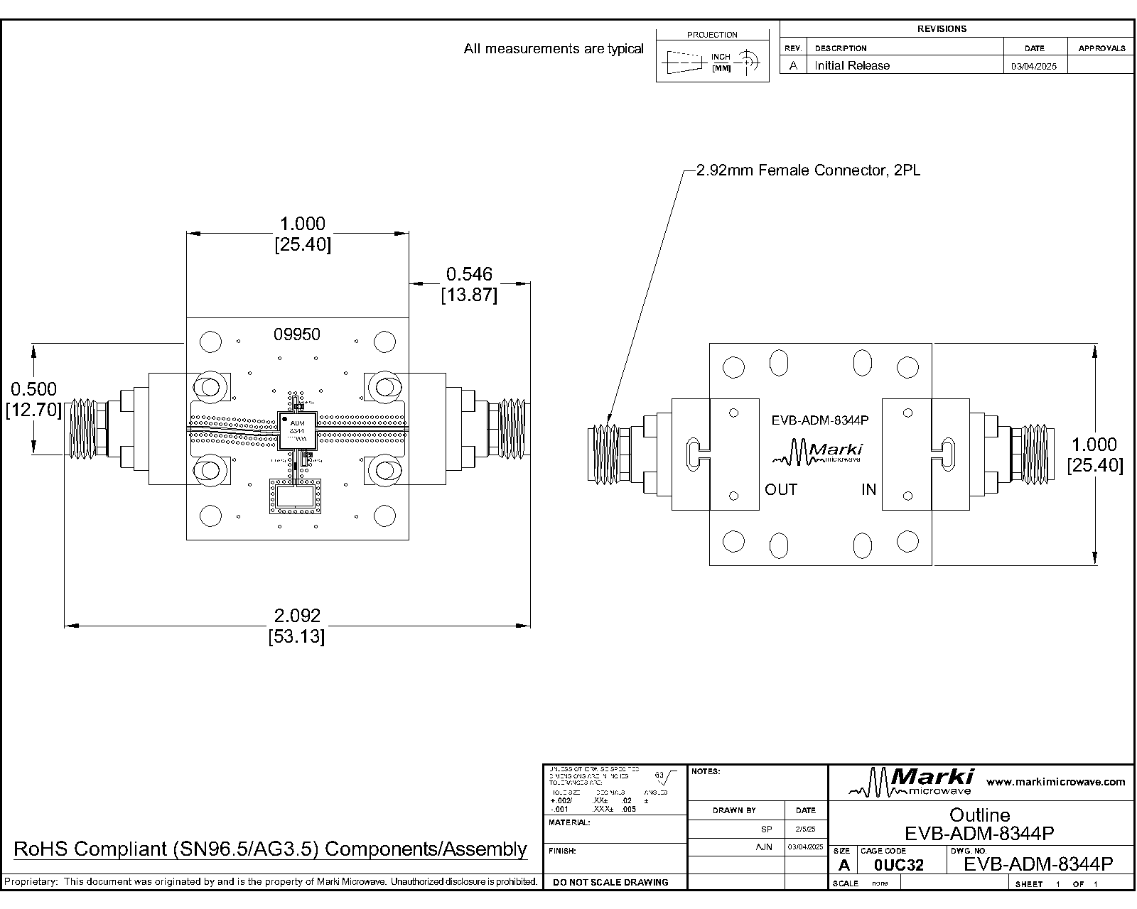
Download : Outline 2D Drawing

Notes (unless otherwise specified):
1. Substrate material is LCP.
2. I/O Leads and Die Paddle is (from base to finish):
Ni: 0.5um MIN
Pd: 0.02um MIN
Au: 0.05um MAX
3. All unconnected pins should be
connected to PCB RF ground.
ADM-8344PSM
DC - 18 GHz Distributed Amplifier
Download : Footprint Drawing

ADM-8344PSM
DC - 18 GHz Distributed Amplifier