Port Diagram
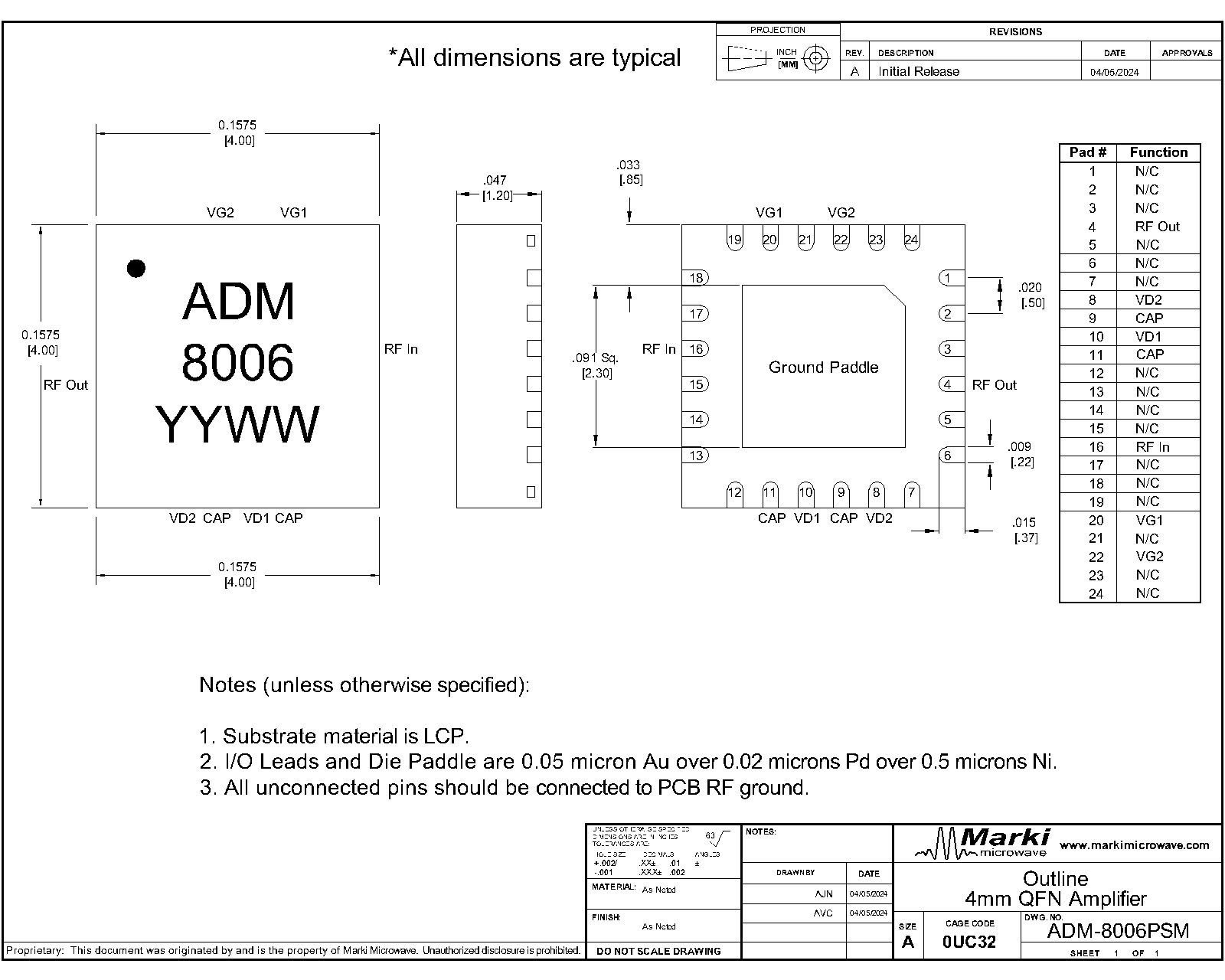
A port diagram of the ADM-8006PSM QFN package is shown below (X-ray view from the top). The pin functions are detailed in this datasheet.

Sales: 408-778-9952 | General: 408-778-4200 | Fax: 408-778-4300
Sales & Customer Support: [email protected]
Tech Support: [email protected]
The ADM-8006PSM is a high-linearity, high gain, low noise distributed amplifier capable of providing +22 dBm output power up to 30 GHz. When driven with an input power of 0 to +5 dBm, the ADM-8006PSM can provide sufficient LO drive to power all H and most S diode mixers to 30GHz. The amplifier has excellent return losses and gain flatness.

| Part Number | Description | Package | Green Status | Product Lifecycle | Export Classification |
|---|---|---|---|---|---|
| ADM-8006PSM | 2 - 30 GHz Surface Mount Amplifier | QFN | REACH RoHS | Released | EAR99 |
| EVB-ADM-8006P | Evaluation Board, 2 - 30 GHz Surface Mount Amplifier | EVB | REACH RoHS | Released | EAR99 |
ADM-8006PSM
2 - 30 GHz Surface Mount Amplifier
| Revision Code | Revision Date | Comment |
|---|---|---|
| G1 | 2024-04-17 | Initial Release |
ADM-8006PSM
2 - 30 GHz Surface Mount Amplifier
A port diagram of the ADM-8006PSM QFN package is shown below (X-ray view from the top). The pin functions are detailed in this datasheet.
ADM-8006PSM
2 - 30 GHz Surface Mount Amplifier
| Port | Function | Description | DC Equivalent Circuit |
|---|---|---|---|
| 10 | Vd1 | Pin 10 is the DC supply pin for the amplifier’s input stage. | - |
| 11 | Cap1 | Pin 11 provides an off-chip AC ground for the input stage. This pin may be left OPEN but should NOT be connected GND. Leaving this pin OPEN will cause some degradation in gain and linearity below 5GHz. | - |
| 1-3, 5-7, 12-15, 17-19, 21, 23, 24 | NC | These pins are not internally connected. Datasheet performance is measured with these pins connected to PCB RF ground. | - |
| 16 | RF Input | Pin 16 is the amplifier RF input. This pin is internally DC blocked and RF matched to 50 Ohms. | - |
| 20 | Vg1 | Pin 20 provides bias for an internal current mirror that sets the current draw for amplifier input stage. Increasing current will increase gain at the expense of efficiency. The default series resistor (270 Ohms) is chosen to optimize gain, output power and efficiency when Vg1 and Vd1 are both tied to 5V. | - |
| 22 | Vg2 | Pin 22 provides bias for an internal current mirror that sets the current draw for amplifier output stage. Increasing current will increase gain at the expense of efficiency. The default series resistor (82.5 Ohms) is chosen to optimize gain, output power and efficiency when Vg2 and Vd2 are both tied to 5V. | - |
| 4 | RF Output | Pin 4 is the amplifier RF output. This pin is internally DC blocked and RF matched to 50 Ohms. | - |
| 8 | Vd2 | Pin 8 is the DC supply pin for the amplifier’s output stage. | - |
| 9 | Cap2 | Pin 9 provides an off-chip AC ground for the output stage. This pin may be left OPEN but should NOT be connected GND. Leaving this pin OPEN will cause some degradation in gain and linearity below 5GHz. | - |
| Paddle | Ground | The package ground paddle must be connected to a DC/RF ground potential with high thermal and electrical conductivity. | - |
ADM-8006PSM
2 - 30 GHz Surface Mount Amplifier
The Absolute Maximum Ratings indicate limits beyond which damage may occur to the device. If any one of these limits are exceeded, the device may become inoperable or have a reduced lifetime. Reliability limits are individual, instantaneous catastrophic limits only. Functional operation limits are indicated below. Operation of the device at multiple absolute maximum limits or for extended periods at a single limit can cause degradation and damage to the device.
| Parameter | Maximum Rating | Unit |
|---|---|---|
| Bias Current (Ig) | 95 | mA |
| Bias Voltage (Vg) | 8 | V |
| Drain Current (Id) | 400 | mA |
| Drain Supply Voltage (Vd) | 8 | V |
| Maximum Operating Temperature for MTTF of 1E6 hours at 85˚C Baseplate Temperature | 85 | °C |
| Maximum Storage Temperature | 125 | °C |
| Max Junction Temperature for MTTF of 1E6 hours at 85˚C Baseplate Temperature | 175 | °C |
| Max Power Dissipation for MTTF of 1E6 hours at 85˚C Baseplate Temperature | 1.6 | W |
| Minimum Operating Temperature for MTTF of 1E6 hours at 85˚C Baseplate Temperature | -40 | °C |
| Minimum Storage Temperature | -65 | °C |
| RF Input Power | 15 | dBm |
| θ_Jc, Junction to Case Thermal Resistance | 30 | ºC/W |
| Parameter | Details | Rating |
|---|---|---|
| ESD | 50 to < 125 Volts | HBM 0A |
| Dimensions | - | 4 x 4 mm |
| Moisture Sensitivity Level | - | MSL 1 |
The Recommended Operating Conditions indicate the limits, inside which the device should be operated, to guarantee the performance given in Electrical Specifications Operating outside these limits may not necessarily cause damage to the device, but the performance may degrade outside the limits of the electrical specifications. For limits, above which damage may occur, see Absolute Maximum Ratings.
| Parameter | Min | Nominal | Max | Unit |
|---|---|---|---|---|
| Power Supply DC Current (Ig) (No RF Input) 1 | 11 | 19 | 23 | mA |
| Power Supply DC Current (Id) (No RF Input) 2 | 121 | 218 | 259 | mA |
| Power Supply DC Voltage (Vd) | 3 | 5 | 6 | V |
| Power Supply DC Voltage (Vg) | 3 | 5 | 6 | V |
| Ambient Temperature | -40 | 25 | 85 | °C |
| Input Power for Saturation | 0 | 2 | 8 | dBm |
[1] Recommended operating current conditions without RF input applied. Bias current into Vg pin.
[2] Recommended operating current conditions without RF input applied. Bias current into Vd pin.
ADM-8006PSM
2 - 30 GHz Surface Mount Amplifier
Unless otherwise specified, electrical specifications apply at TA=+25°C, Vd1,Vd2,Vg1,Vg2 = 5 V. Typical performance data is measure on an EVB unless otherwise stated. Min and Max limits are guaranteed at TA=+25°C.
| Parameter | Test Conditions | Minimum Frequency (GHz) | Maximum Frequency (GHz) | Min | Typ | Max | Unit |
|---|---|---|---|---|---|---|---|
| Current Consumption | Vd1, Vd2, Vg1, Vg2 = 5 V no RF input | - | - | - | 237 | - | mA |
| Input IP3 | Vd1, Vd2, Vg1, Vg2 = 5 V Pin = -15 dBm per tone, 10 MHz tone spacing | 2 | 30 | - | 9 | - | dBm |
| Input Power for Saturation | Vd1, Vd2, Vg1, Vg2 = 5 V | 2 | 30 | - | 2 | - | dBm |
| Input Return Loss | Vd1, Vd2, Vg1, Vg2 = 5 V Pin = -20 dBm | 2 | 30 | - | 22 | - | dB |
| Noise Figure | Vd1, Vd2, Vg1, Vg2 = 5 V Pin = -20 dBm | 2 | 30 | - | 2.7 | - | dB |
| Output IP2 | Vd1, Vd2, Vg1, Vg2 = 5 V Pin = -15 dBm per tone, 10 MHz tone spacing | 2 | 12 | - | 45 | - | dBm |
| Output IP2 | Vd1, Vd2, Vg1, Vg2 = 5 V Pin = -15 dBm per tone, 10 MHz tone spacing | 12 | 22 | - | 37 | - | dBm |
| Output IP3 | Vd1, Vd2, Vg1, Vg2 = 5 V Pin = -15 dBm per tone, 10 MHz tone spacing | 2 | 30 | - | 30 | - | dBm |
| Output P1dB | Vd1, Vd2, Vg1, Vg2 = 5 V | 2 | 30 | - | 21 | - | dBm |
| Output Return Loss | Vd1, Vd2, Vg1, Vg2 = 5 V Pin = -20 dBm | 2 | 30 | - | 17 | - | dB |
| Reverse Isolation | Vd1, Vd2, Vg1, Vg2 = 5 V Pin = -20 dBm | 2 | 30 | - | 60 | - | dB |
| Saturated Output Power | Vd1, Vd2, Vg1, Vg2 = 5 V | 2 | 30 | - | 23 | - | dBm |
| Small Signal Gain | Vd1, Vd2, Vg1, Vg2 = 5 V Pin = -20 dBm | 2 | 30 | - | 23 | - | dB |
ADM-8006PSM
2 - 30 GHz Surface Mount Amplifier


ADM-8006PSM
2 - 30 GHz Surface Mount Amplifier


ADM-8006PSM
2 - 30 GHz Surface Mount Amplifier
ADM-8006PSM
2 - 30 GHz Surface Mount Amplifier
Download : Footprint Drawing

ADM-8006PSM
2 - 30 GHz Surface Mount Amplifier