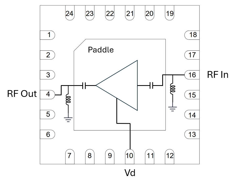
Port Diagram
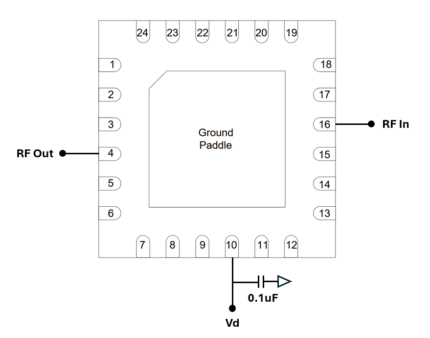
A port diagram of the ADM-11425PSM QFN is shown below (X-ray view from the bottom).
Sales: 408-778-9952 | General: 408-778-4200 | Fax: 408-778-4300
Sales & Customer Support: [email protected]
Tech Support: [email protected]
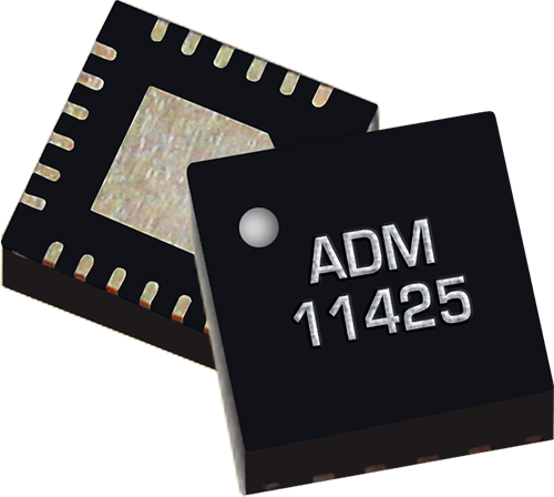
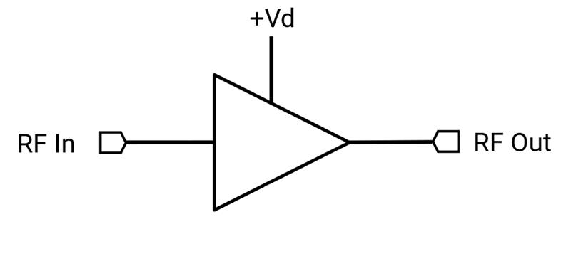
The ADM-11425PSM is a broadband gain block amplifier delivering 23 dB of gain across a wide bandwidth. Fabricated on a GaAs pHEMT process, it operates from a single +5V supply with no negative bias or bias sequencing required, and features a minimal application circuit that simplifies board-level integration. The device is housed in a compact 4mm plastic QFN package for surface mount assembly.
| Part Number | Description | Package | Green Status | Product Lifecycle | Export Classification |
|---|---|---|---|---|---|
| ADM-11425PSM | 4 - 40GHz Broadband, Gain Block Amplifier | Plastic QFN | REACH RoHS | Released | 3A001.b.2.d |
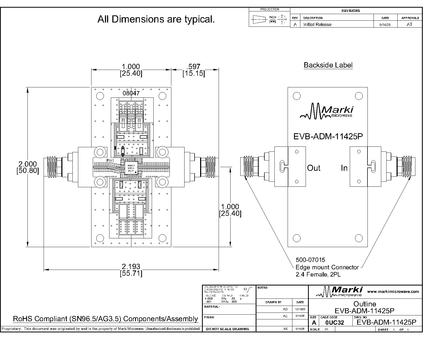
| EVB-ADM-11425P | Evaluation Board, 4 - 40GHz Broadband, Gain Block Amplifier | EVB | REACH RoHS | Released | EAR99 |
| Part Number | Description | Package | Green Status | Product Lifecycle | Export Classification |
|---|---|---|---|---|---|
| ADM-11425PSM | 4 - 40GHz Broadband, Gain Block Amplifier | Plastic QFN | REACH RoHS | Released | 3A001.b.2.d |
| EVB-ADM-11425P | Evaluation Board, 4 - 40GHz Broadband, Gain Block Amplifier | EVB | REACH RoHS | Released | EAR99 |
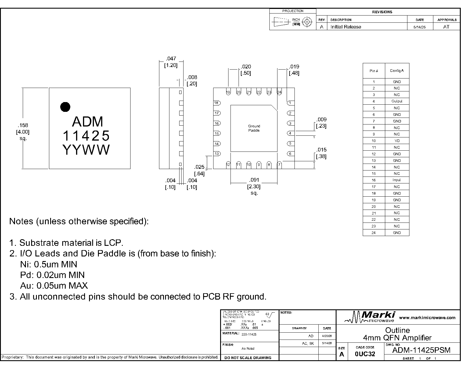
ADM-11425PSM
4 - 40GHz Broadband, Gain Block Amplifier
| Revision Code | Revision Date | Comment |
|---|---|---|
| - | 2026-06-19 | Initial Release |
ADM-11425PSM
4 - 40GHz Broadband, Gain Block Amplifier
A port diagram of the ADM-11425PSM QFN is shown below (X-ray view from the bottom).
| Port | Function | Description | DC Equivalent Circuit |
|---|---|---|---|
| GND | Ground | IC backside must be connected to a DC/RF ground with high thermal and electrical conductivity. |  |
| Pin 10 | Vd | Pin 10 is the DC bias supply for the amplifier. The voltage at this pin should be set to 5V for normal operation. This part requires an off-chip bypass capacitor of 0.1uF installed at this pin as close to the IC as possible. See applications circuit. |  |
| Pin 16 | RF Input | Pin 16 is the amplifier's RF input pin. This port is internally matched to 50 Ohms and is internally DC shorted to GND. No DC block is required for operation if no DC is present on the line but should be DC blocked otherwise. |  |
| Pin 4 | RF Output | Pin 4 is the amplifier's RF output pin. This port is internally matched to 50 Ohms and is internally DC shorted to GND. No DC block is required for operation if no DC is present on the line but should be DC blocked otherwise. | |
ADM-11425PSM
4 - 40GHz Broadband, Gain Block Amplifier
The Absolute Maximum Ratings indicate limits beyond which damage may occur to the device. If these limits are exceeded, the device may be inoperable or have a reduced lifetime. This amplifier is designed and characterized in a 50Ω system, and operation in a reflective environment can cause performance degradation.
| Parameter | Maximum Rating | Unit |
|---|---|---|
| Maximum Operating Temperature | 85 | °C |
| Maximum Storage Temperature | 125 | °C |
| Max Junction Temperature for MTTF > 1E6 hours | 175 | °C |
| Minimum Operating Temperature | -54 | °C |
| Minimum Storage Temperature | -65 | °C |
| Positive Drain Supply Voltage (Vd) | 6 | V |
| RF Input Power | 18 | dBm |
| Thermal Resistance, θJC | 19.5 | ºC/W |
| Total Positive Drain Supply Current (Id) | 150 | mA |
| Parameter | Details | Rating |
|---|---|---|
| ESD | 250 to < 500 Volts | HBM Class 1A |
| Weight | Package name: Plastic QFN | 0.041g |
| Dimensions | - | 4 x 4 mm |
| Moisture Sensitivity Level | - | MSL 1 |
The Recommended Operating Conditions indicate the limits, inside which the device should be operated, to guarantee the performance given in Electrical Specifications. Operating outside these limits may not necessarily cause damage to the device, but the performance may degrade outside the limits of the Electrical Specifications. For limits, above which damage may occur, see Absolute Maximum Ratings.
| Parameter | Min | Nominal | Max | Unit |
|---|---|---|---|---|
| Power Supply DC Voltage | 4 | 5 | 6 | V |
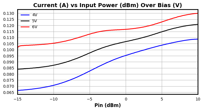
| Positive DC Current (Id) (No RF Input) | - | 85 | - | mA |
| Ambient Temperature | -55 | 25 | 85 | °C |
ADM-11425PSM
4 - 40GHz Broadband, Gain Block Amplifier
Unless otherwise specified, electrical specifications apply at TA=+25°C, Vd = 5 V, and Id = 85mA in a 50Ω system. QFNs are 100% RF tested.
| Parameter | Test Conditions | Minimum Frequency (GHz) | Maximum Frequency (GHz) | Min | Typ | Max | Unit |
|---|---|---|---|---|---|---|---|
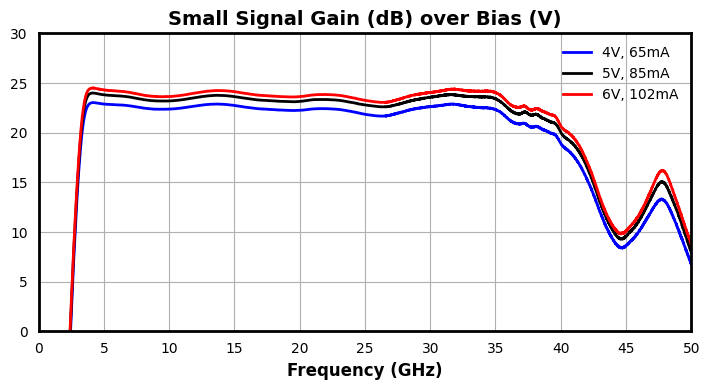
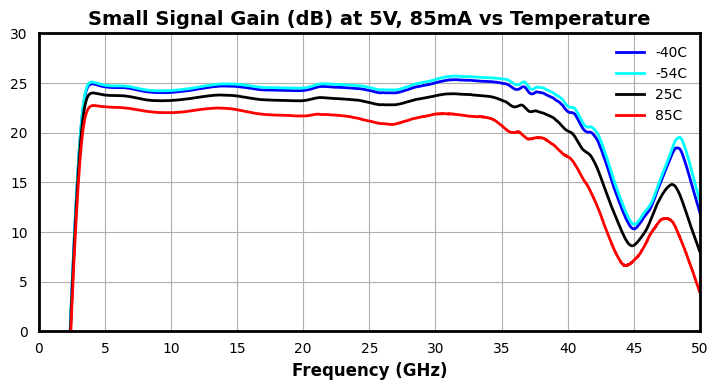
| Small Signal Gain | Pin = -15 dBm, Vd = 5V, Id = 85 mA | 4 | 40 | - | 23.0 | - | dB |
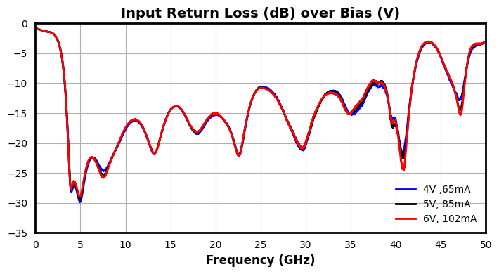
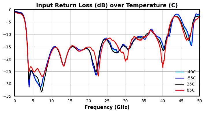
| Input Return Loss | Pin = -15 dBm, Vd = 5V, Id = 85 mA | 4 | 40 | - | 16 | - | dB |
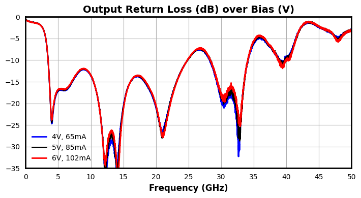
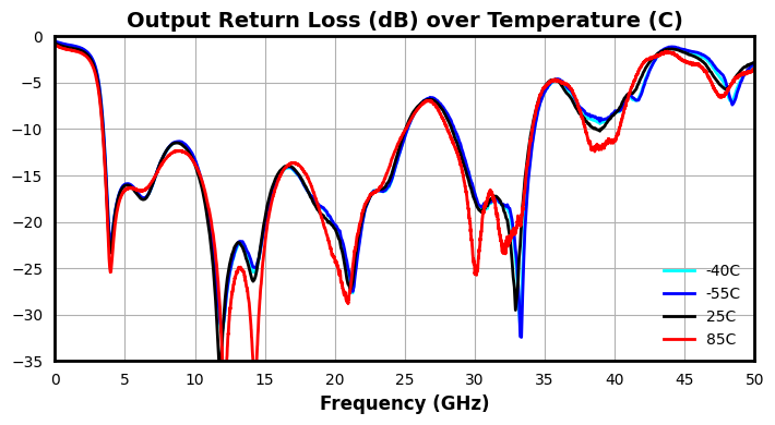
| Output Return Loss | Pin = -15 dBm, Vd = 5V, Id = 85 mA | 4 | 40 | - | 15 | - | dB |
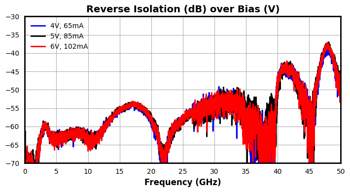
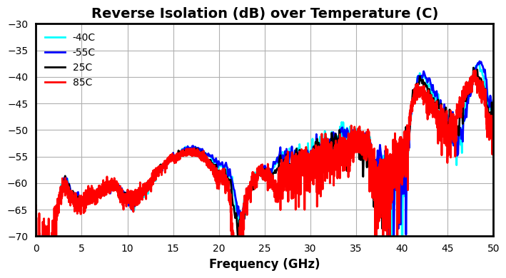
| Reverse Isolation | Pin = -15 dBm, Vd = 5V, Id = 85 mA | 4 | 40 | - | 58 | - | dB |
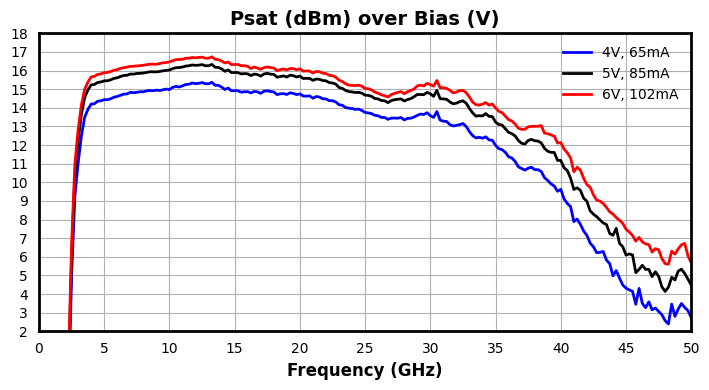
| Saturated Output Power | Vd = 5V, Id = 85 mA | 4 | 40 | - | 15.1 | - | dBm |
| Input P1dB | Vd = 5V, Id = 85 mA | 4 | 40 | - | -11.5 | - | dBm |
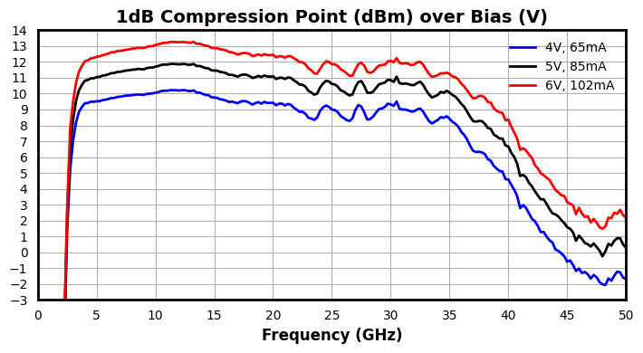
| Output P1dB | Vd = 5V, Id = 85 mA | 4 | 40 | - | 10.5 | - | dBm |
| Input IP3 | Pin = -18 dBm, Vd = 5V, Id = 85 mA, 1 MHz Tone Spacing | 4 | 40 | - | 3 | - | dBm |
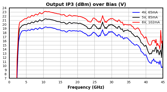
| Output IP3 | Pin = -18 dBm, Vd = 5V, Id = 85 mA, 1 MHz Tone Spacing | 4 | 40 | - | 19.5 | - | dBm |
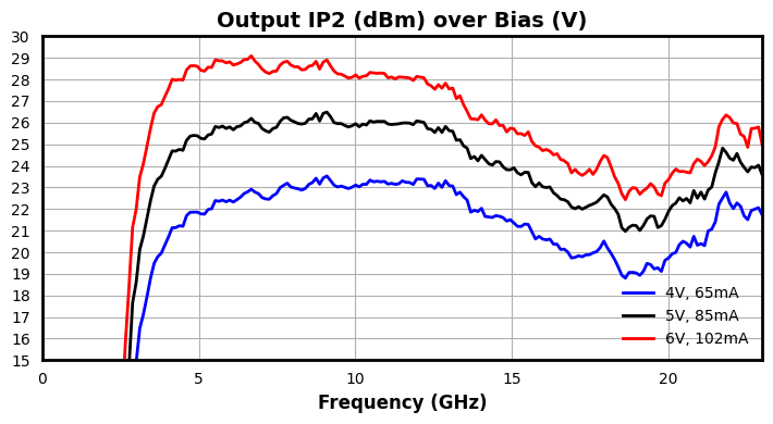
| Input IP2 | Pin = -22 dBm, Vd = 5V, Id = 85 mA, 1 MHz Tone Spacing | 4 | 40 | - | 0.5 | - | dBm |
| Output IP2 | Pin = -22 dBm, Vd = 5V, Id = 85 mA, 1 MHz Tone Spacing | 4 | 40 | - | 23 | - | dBm |
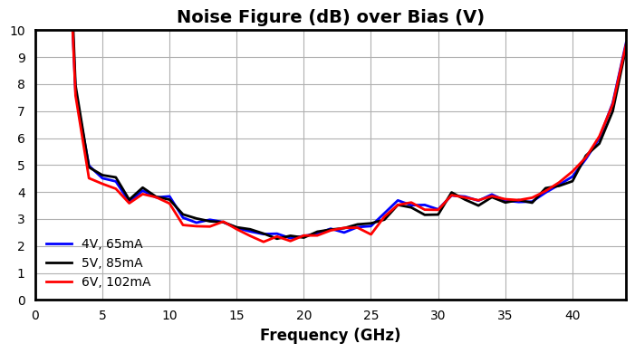
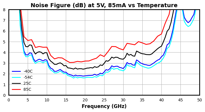
| Noise Figure | Vd = 5V, Id = 85 mA | 4 | 40 | - | 3.3 | - | dB |
| Parameter | Test Conditions | Minimum Frequency (GHz) | Maximum Frequency (GHz) | Min | Typ | Max | Unit |
|---|---|---|---|---|---|---|---|
| Small Signal Gain | Pin = -15 dBm, Vd = 5V, Id = 85 mA | 4 | 40 | - | 23.0 | - | dB |
| Input Return Loss | Pin = -15 dBm, Vd = 5V, Id = 85 mA | 4 | 40 | - | 16 | - | dB |
| Output Return Loss | Pin = -15 dBm, Vd = 5V, Id = 85 mA | 4 | 40 | - | 15 | - | dB |
| Reverse Isolation | Pin = -15 dBm, Vd = 5V, Id = 85 mA | 4 | 40 | - | 58 | - | dB |
| Saturated Output Power | Vd = 5V, Id = 85 mA | 4 | 40 | - | 15.1 | - | dBm |
| Input P1dB | Vd = 5V, Id = 85 mA | 4 | 40 | - | -11.5 | - | dBm |
| Output P1dB | Vd = 5V, Id = 85 mA | 4 | 40 | - | 10.5 | - | dBm |
| Input IP3 | Pin = -18 dBm, Vd = 5V, Id = 85 mA, 1 MHz Tone Spacing | 4 | 40 | - | 3 | - | dBm |
| Output IP3 | Pin = -18 dBm, Vd = 5V, Id = 85 mA, 1 MHz Tone Spacing | 4 | 40 | - | 19.5 | - | dBm |
| Input IP2 | Pin = -22 dBm, Vd = 5V, Id = 85 mA, 1 MHz Tone Spacing | 4 | 40 | - | 0.5 | - | dBm |
| Output IP2 | Pin = -22 dBm, Vd = 5V, Id = 85 mA, 1 MHz Tone Spacing | 4 | 40 | - | 23 | - | dBm |
| Noise Figure | Vd = 5V, Id = 85 mA | 4 | 40 | - | 3.3 | - | dB |
ADM-11425PSM
4 - 40GHz Broadband, Gain Block Amplifier
ADM-11425PSM
4 - 40GHz Broadband, Gain Block Amplifier
ADM-11425PSM
4 - 40GHz Broadband, Gain Block Amplifier
ADM-11425PSM
4 - 40GHz Broadband, Gain Block Amplifier
ADM-11425PSM
4 - 40GHz Broadband, Gain Block Amplifier
ADM-11425PSM
4 - 40GHz Broadband, Gain Block Amplifier
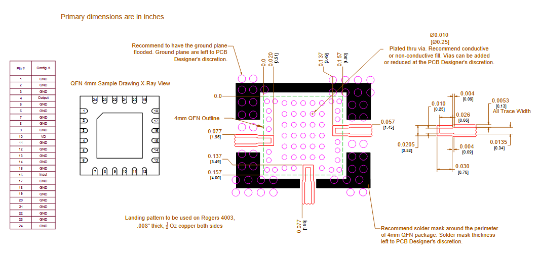
Download : Footprint Drawing
ADM-11425PSM
4 - 40GHz Broadband, Gain Block Amplifier