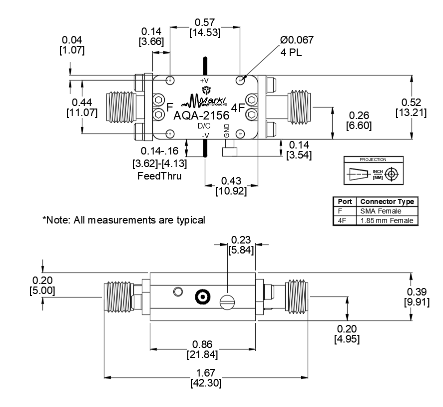
Port Diagram


Sales: 408-778-9952 | General: 408-778-4200 | Fax: 408-778-4300
Sales & Customer Support: [email protected]
Tech Support: [email protected]
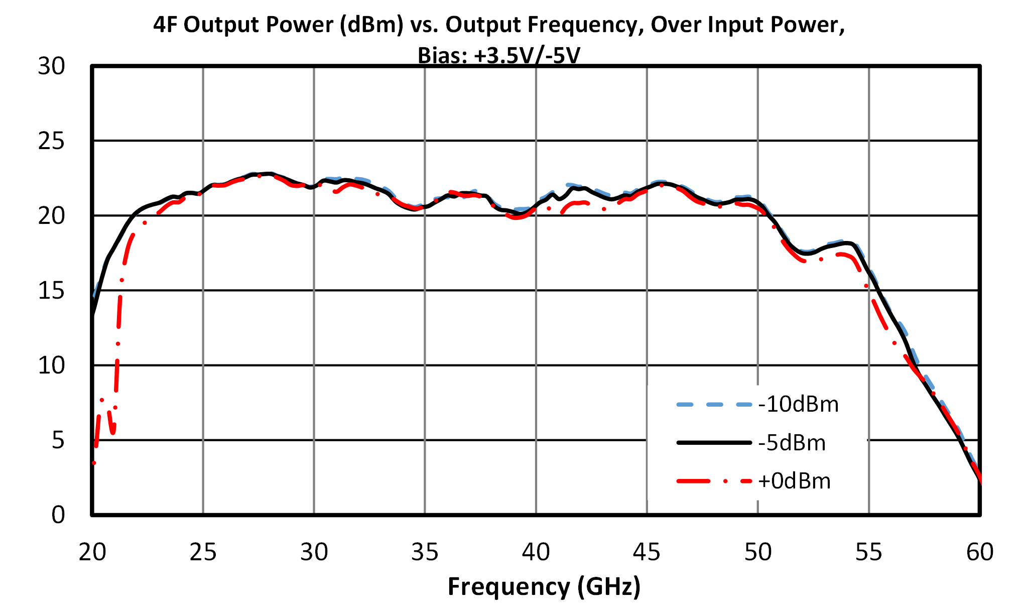
The AQA-2156 is an amplified frequency multiplier that quadruples the 5.25 – 14 GHz input frequency, producing an amplified 21 - 56 GHz quadrupled output frequency. This multiplier is designed to provide +20 dBm 4F output power with +0 dBm input power and offers superior harmonic suppressions. It can provide sufficient LO drive for Marki S-, H-, and L- diode mixers.


| Part Number | Description | Connectors | Green Status | Product Lifecycle | Export Classification |
|---|---|---|---|---|---|
| AQA-2156 | 21-56 GHz Amplified 4F Multiplier | Standard | RoHS REACH | Released | EAR99 |
| Part Number | Description | Connectors | Green Status | Product Lifecycle | Export Classification |
|---|---|---|---|---|---|
| AQA-2156 | 21-56 GHz Amplified 4F Multiplier | Standard | RoHS REACH | Released | EAR99 |
AQA-2156
21-56 GHz Amplified 4F Multiplier
| Revision Code | Revision Date | Comment |
|---|---|---|
| - | 2020-04-01 | Initial Release Datasheet |
| A | 2020-07-01 | Updated Min Output Power and Suppression Specs |
| B | 2020-08-01 | Inclusion of internal chipset |
| C | 2020-10-01 | Adjusted Build to Reduce Power Dissipation, Updated Bias Condition, Updated Absolute Maximum Specifications, Updated Performance Plots |
| D | 2021-07-01 | Adjusted Build to Reduce Power Dissipation, Updated Bias Condition, Updated Absolute Maximum Specifications, Updated Performance Plots |
| E | 2023-03-01 | Adjusted Build, Updated Electrical Specifications and Performance Plots |
AQA-2156
21-56 GHz Amplified 4F Multiplier
| Port | Function | Connector Type | Description | DC Equivalent Circuit |
|---|---|---|---|---|
| Bias | Negative bias | - | Gate control for the amplifier must be connected to a -5.0 to -6.0 Volt power supply. | 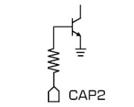 |
| GND | Ground | - | Ground path is provided through the metal housing and outer ground lug. |  |
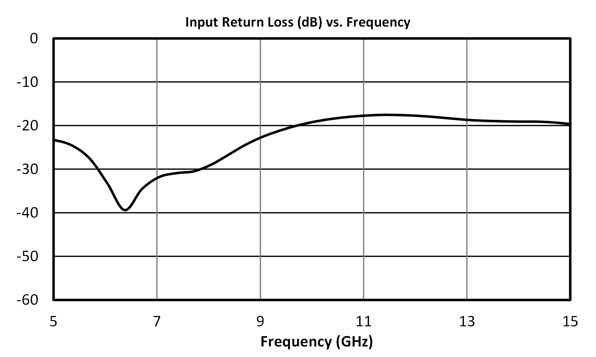
| Port 1 | Input | SMAF | This pin is for the RF input. It is internally DC-blocked and is matched to 50 ohms from 5.25-14 GHz. |  |
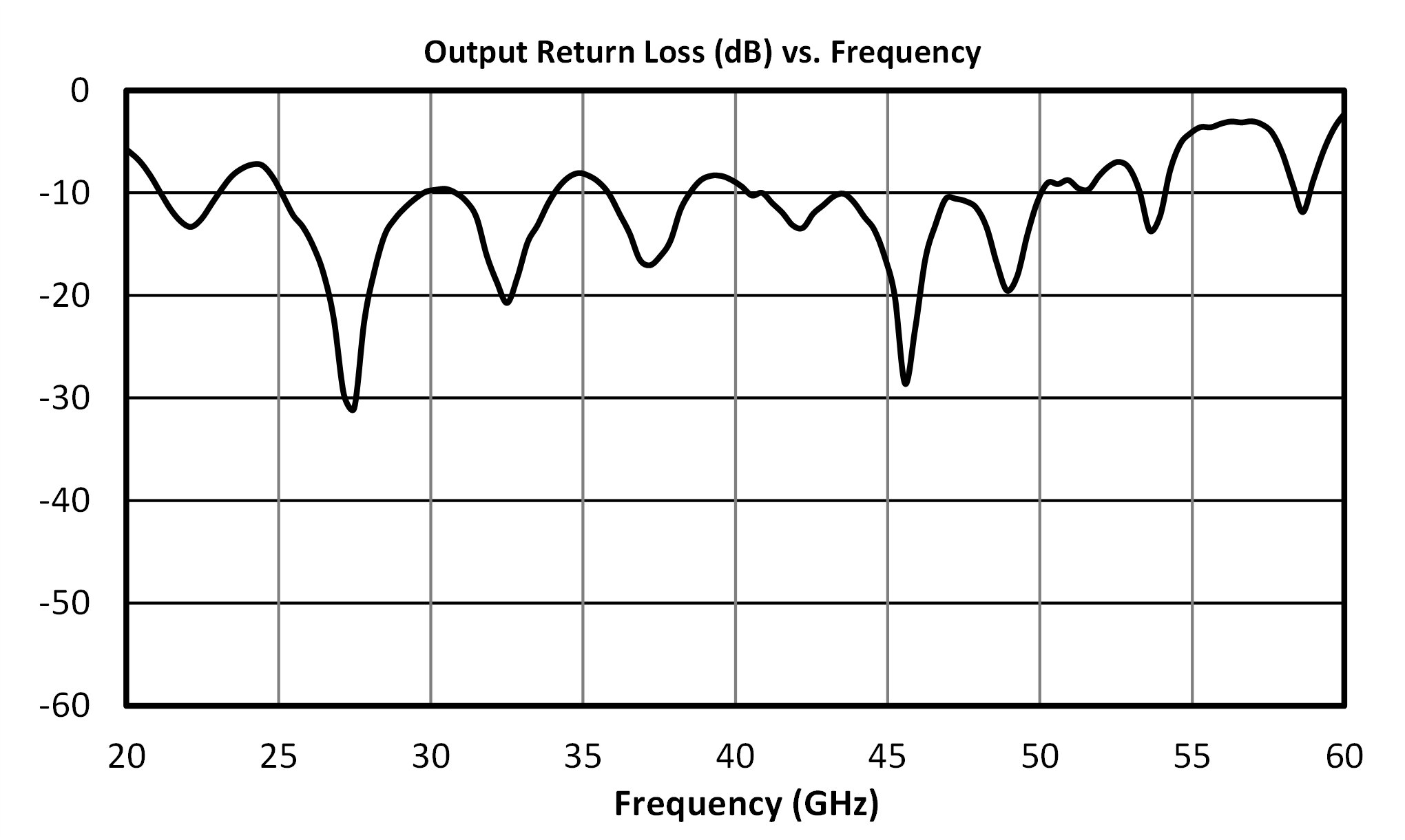
| Port 2 | Output | 1.85F | This pin is for the RF output. It is internally DC-blocked matched to 50 ohms from 21-56 GHz. | |
| Power Supply | Positive bias | - | Positive bias port must be connected to a +3V to +3.5V power supply. |  |
AQA-2156
21-56 GHz Amplified 4F Multiplier
The Absolute Maximum Ratings indicate limits beyond which damage may occur to the device. If these limits are exceeded, the device may be inoperable or have a reduced lifetime.
| Parameter | Maximum Rating | Unit |
|---|---|---|
| Maximum Operating Temperature | 50 | °C |
| Maximum Storage Temperature | 150 | °C |
| Minimum Operating Temperature | -40 | °C |
| Minimum Storage Temperature | -65 | °C |
| Negative Bias Current | 3 | mA |
| Negative Bias Voltage | -10 | V |
| Positive Bias Current | 800 | mA |
| Positive Bias Voltage | 4 | V |
| RF Input Power | 5 | dBm |
| Parameter | Details | Rating |
|---|---|---|
| ESD | 250 to < 500 Volts | HBM Class 1A |
| Dimensions | - | 21.84 x 13.21 mm |
AQA-2156
21-56 GHz Amplified 4F Multiplier
The electrical specifications apply at TA=+25°C in a 50Ω system.
| Parameter | Test Conditions | Minimum Frequency (GHz) | Maximum Frequency (GHz) | Min | Typ | Max | Unit |
|---|---|---|---|---|---|---|---|
| 4F Output Power | Input = 12 – 14 GHz Output = 48 - 56 GHz | - | - | - | 18 | - | dBm |
| 4F Output Power | Input = 5.25 – 6.25 GHz Output = 21 - 25 GHz | - | - | - | 20 | - | dBm |
| 4F Output Power | Input = 6.25 – 12 GHz Output = 25 - 48 GHz | - | - | 17 | 21 | - | dBm |
| Current Consumption 1 | 3.5 Volts DC | - | - | - | 250 | - | mA |
| Current Consumption 2 | -5.0 Volts DC | - | - | - | 10 | - | mA |
| Input Frequency Range | - | - | - | 5.25 | - | 14 | GHz |
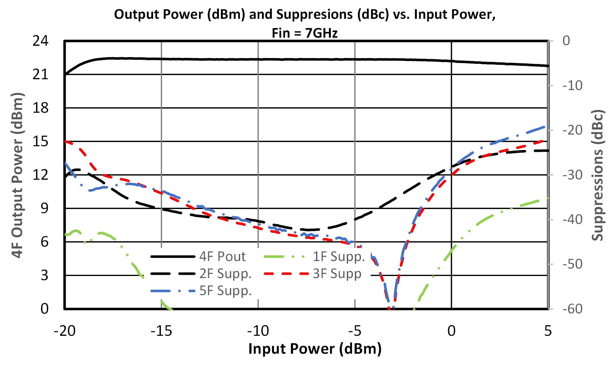
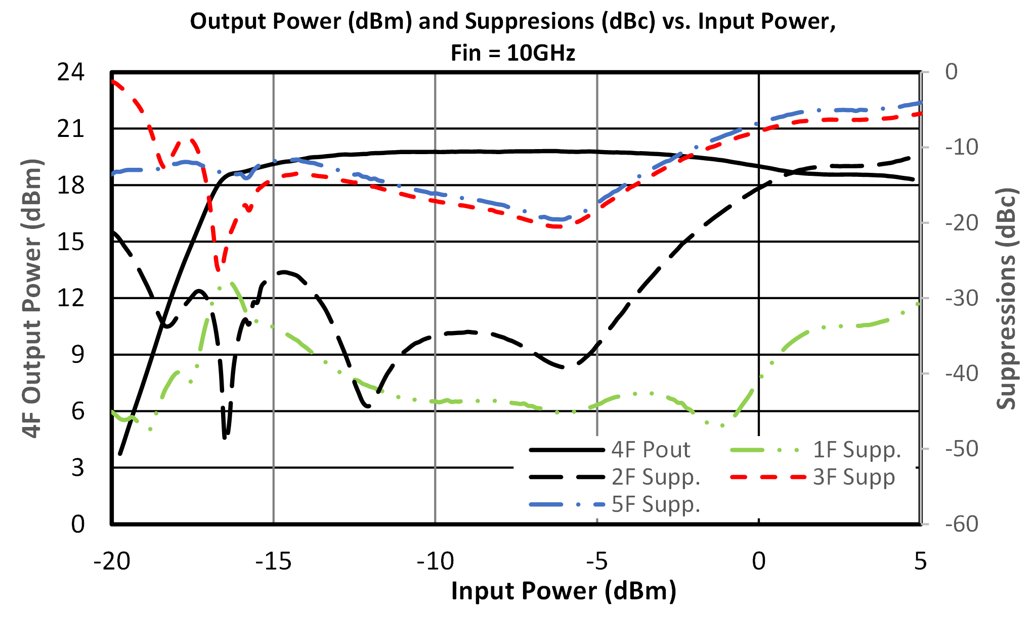
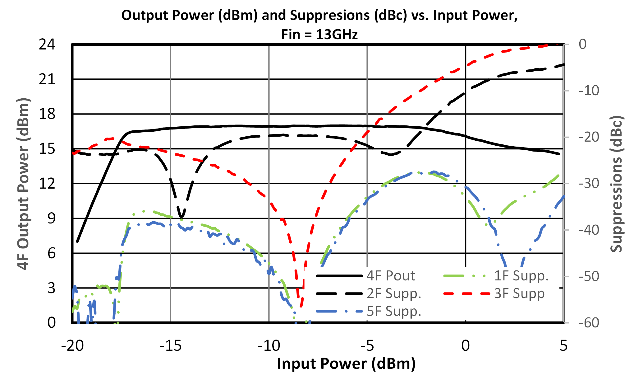
| Input Power 3 | - | - | - | -10 | -5 | 0 | dBm |
| Output Frequency Range | - | - | - | 21 | - | 56 | GHz |
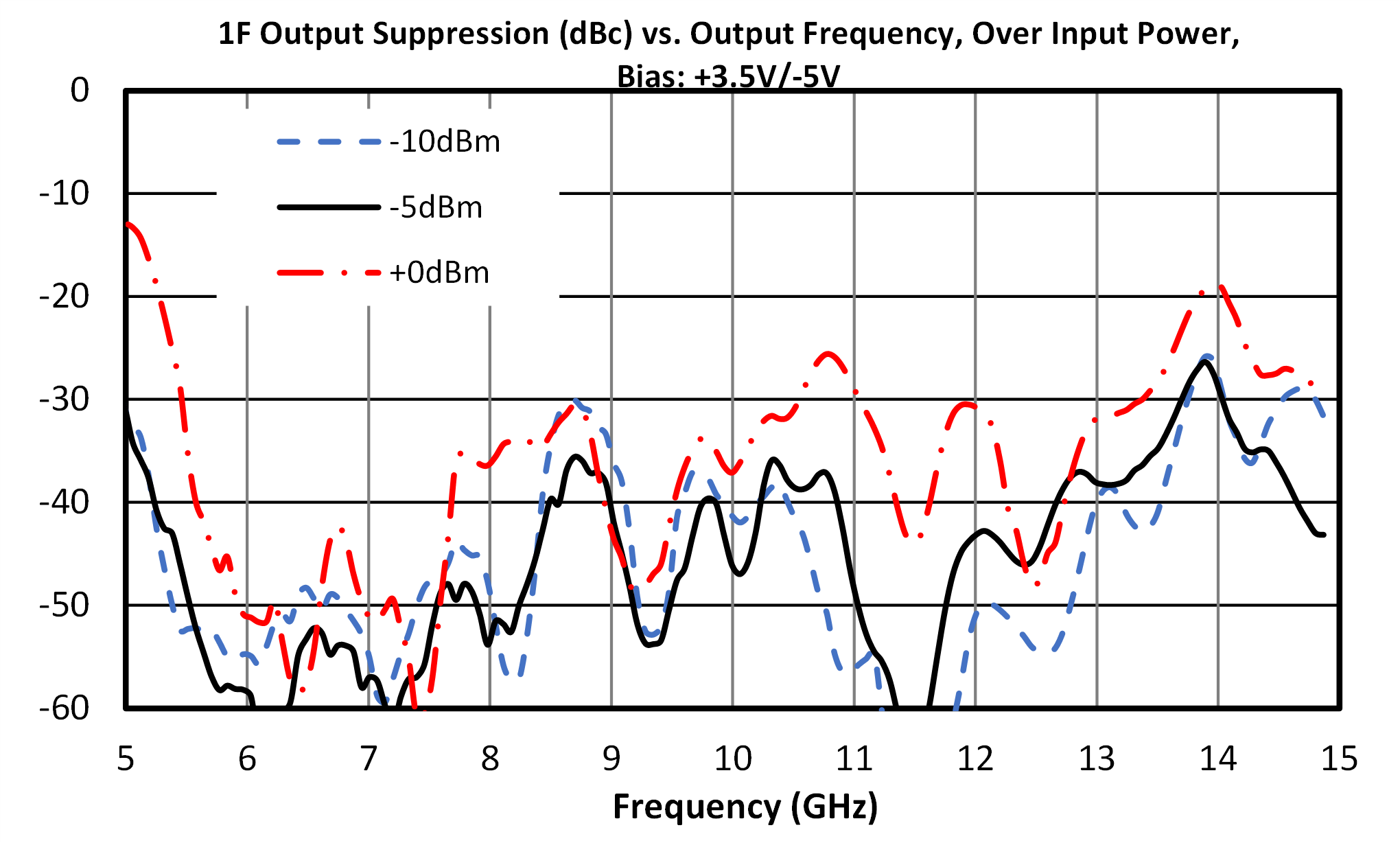
| Suppression, 1F 4 | Input = 5.25 – 14 GHz Output = 5.25 – 14 GHz | - | - | - | 44 | - | dBc |
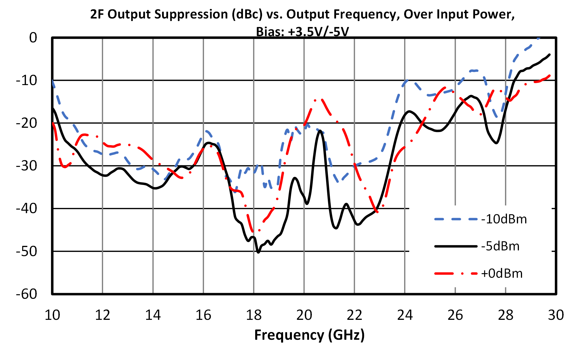
| Suppression, 2F 5 | Input = 5.25 – 14 GHz Output = 10.5 - 28 GHz | - | - | - | 35 | - | dBc |
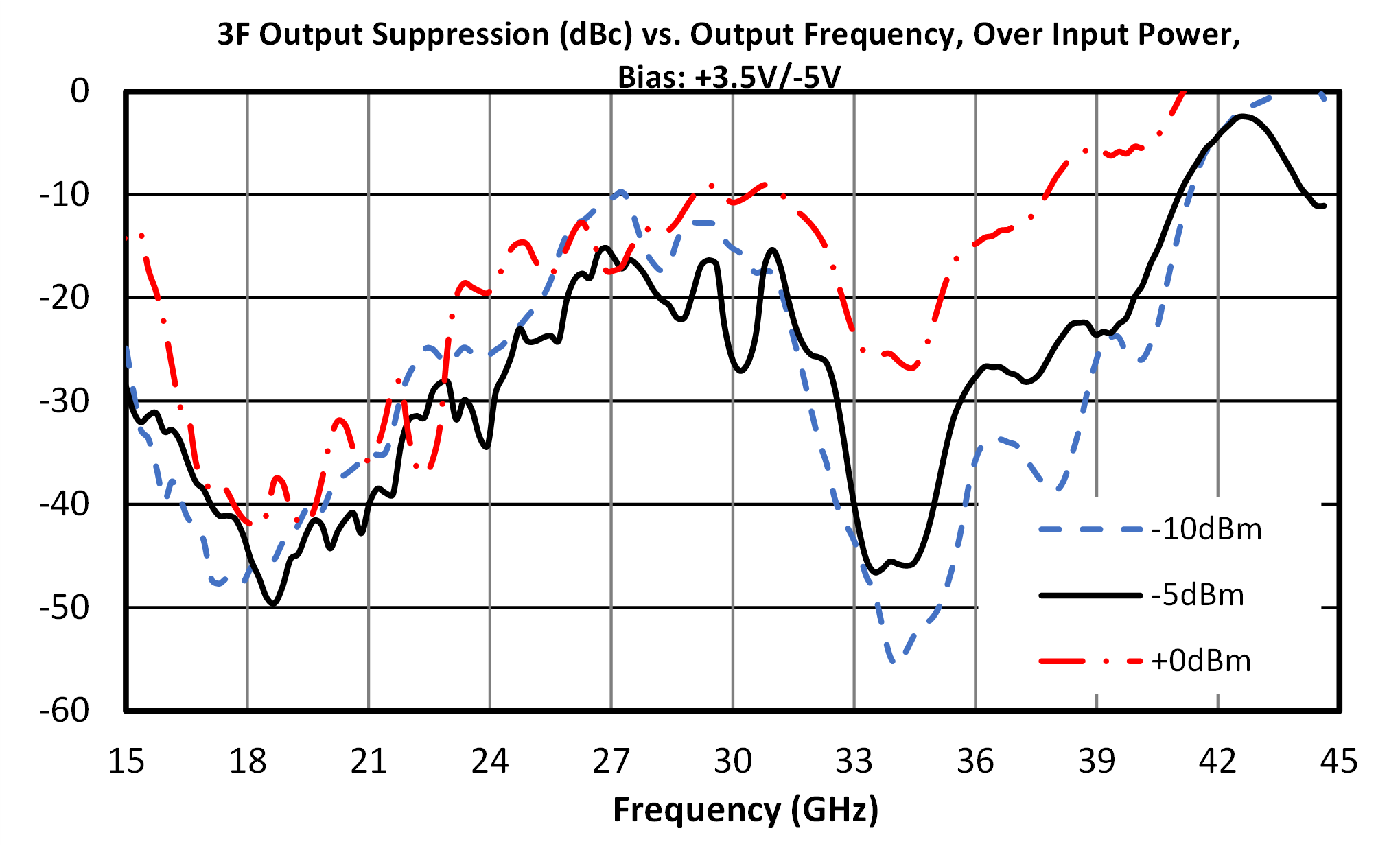
| Suppression, 3F 6 | Input = 5.25 – 14 GHz Output = 15.75 - 42 GHz | - | - | - | 24 | - | dBc |
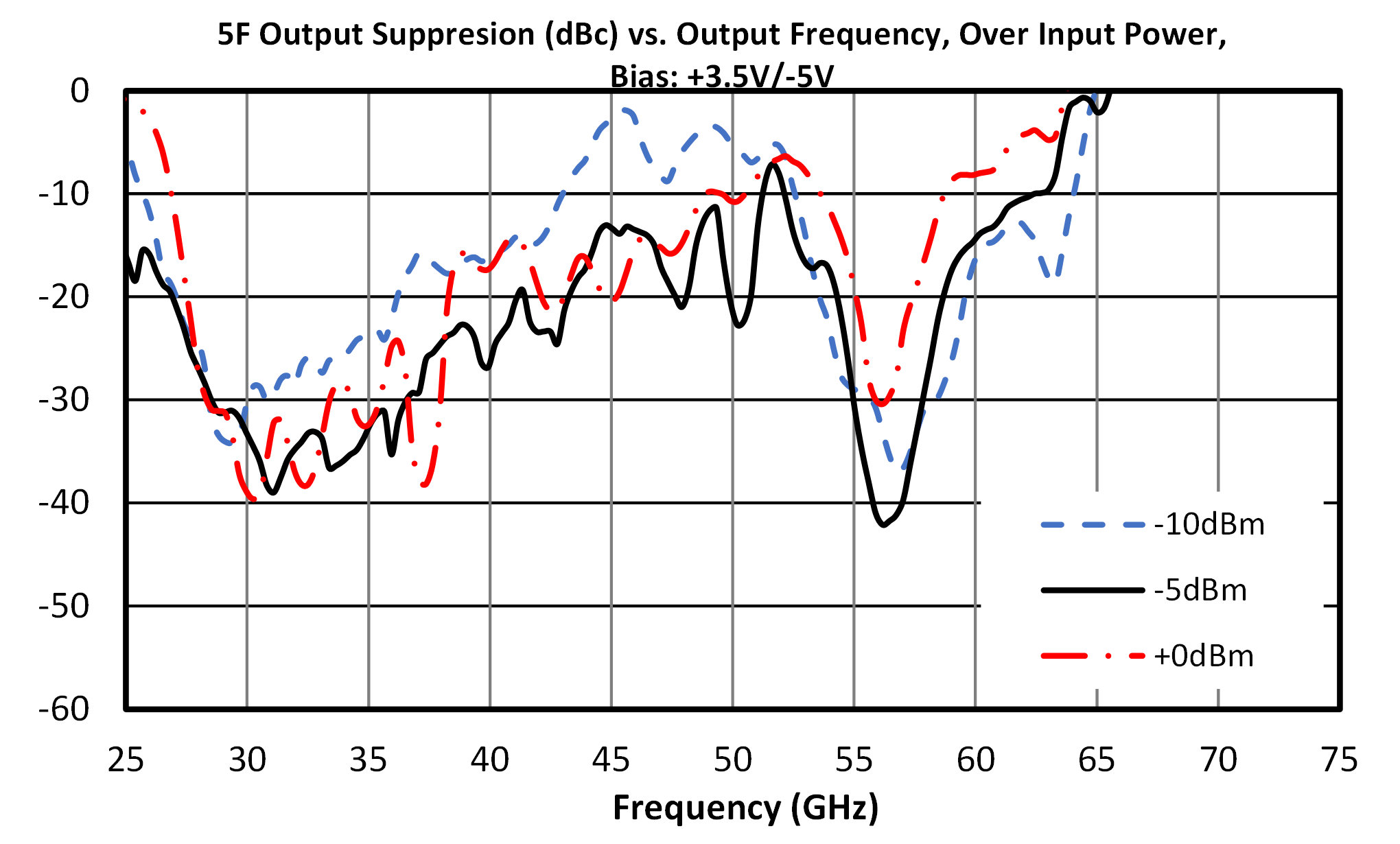
| Suppression, 5F 7 | Input = 5.25 – 13.4 GHz Output = 26.25 - 67 GHz | - | - | - | 32 | - | dB |
| Parameter | Test Conditions | Minimum Frequency (GHz) | Maximum Frequency (GHz) | Min | Typ | Max | Unit |
|---|---|---|---|---|---|---|---|
| 4F Output Power | Input = 12 – 14 GHz Output = 48 - 56 GHz | - | - | - | 18 | - | dBm |
| 4F Output Power | Input = 5.25 – 6.25 GHz Output = 21 - 25 GHz | - | - | - | 20 | - | dBm |
| 4F Output Power | Input = 6.25 – 12 GHz Output = 25 - 48 GHz | - | - | 17 | 21 | - | dBm |
| Current Consumption 1 | 3.5 Volts DC | - | - | - | 250 | - | mA |
| Current Consumption 2 | -5.0 Volts DC | - | - | - | 10 | - | mA |
| Input Frequency Range | - | - | - | 5.25 | - | 14 | GHz |
| Input Power 3 | - | - | - | -10 | -5 | 0 | dBm |
| Output Frequency Range | - | - | - | 21 | - | 56 | GHz |
| Suppression, 1F 4 | Input = 5.25 – 14 GHz Output = 5.25 – 14 GHz | - | - | - | 44 | - | dBc |
| Suppression, 2F 5 | Input = 5.25 – 14 GHz Output = 10.5 - 28 GHz | - | - | - | 35 | - | dBc |
| Suppression, 3F 6 | Input = 5.25 – 14 GHz Output = 15.75 - 42 GHz | - | - | - | 24 | - | dBc |
| Suppression, 5F 7 | Input = 5.25 – 13.4 GHz Output = 26.25 - 67 GHz | - | - | - | 32 | - | dB |
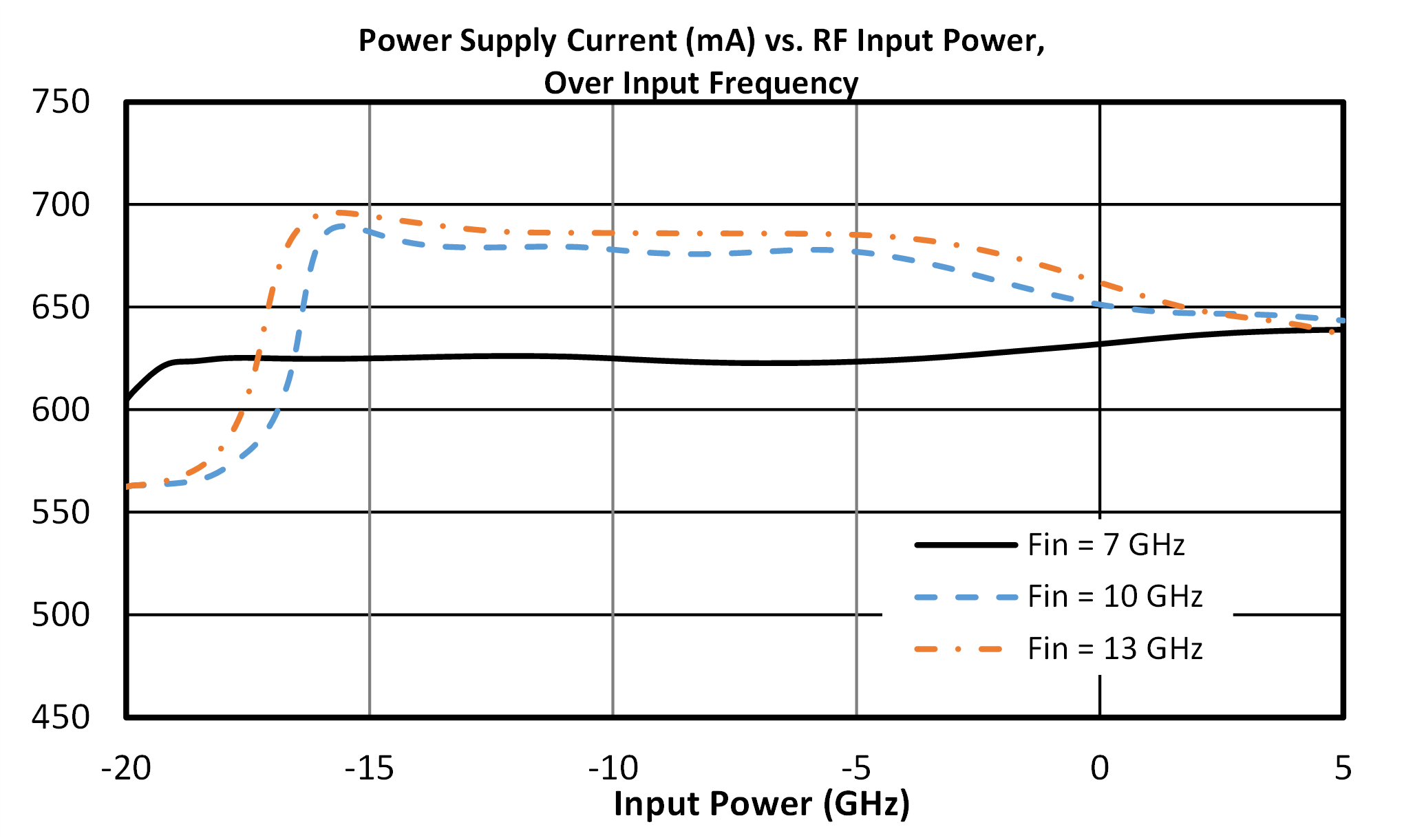
[1][2] Current consumption taken under NO RF input power. Current draw will increase with increased input power. Optimal Performance is at approximately +3.5V / -5.0V.
[3] Optimal suppression levels at -10 - 0 dBm input power.
[4][5][6][7] Suppression is defined as the harmonic power relative to the 4F quadrupled output power.
AQA-2156
21-56 GHz Amplified 4F Multiplier
AQA-2156
21-56 GHz Amplified 4F Multiplier
AQA-2156
21-56 GHz Amplified 4F Multiplier