Port Diagram
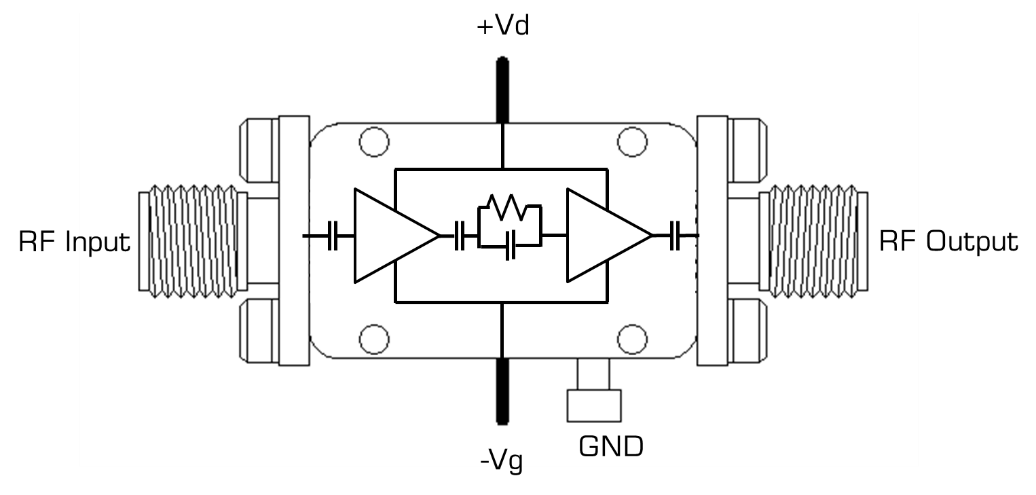
A top-down port diagram of the ADM2-0035PA’s connectorized package is shown below.

Sales: 408-778-9952 | General: 408-778-4200 | Fax: 408-778-4300
Sales & Customer Support: [email protected]
Tech Support: [email protected]
The ADM2-0035PA is an LO driver amplifier module with 2 internally connected wideband gain stages and equalization. It is designed to provide sufficient gain and output power for Marki S-diode mixers below 35 GHz with an input power of 0-5 dBm.

| Part Number | Description | Package | Connectors | Green Status | Product Lifecycle | Export Classification |
|---|---|---|---|---|---|---|
| ADM2-0035PA | 0.1-35 GHz 2-Stage LO Driver Amplifier | PA | Standard | REACH RoHS | Released | EAR99 |
| Part Number | Description | Package | Connectors | Green Status | Product Lifecycle | Export Classification |
|---|---|---|---|---|---|---|
| ADM2-0035PA | 0.1-35 GHz 2-Stage LO Driver Amplifier | PA | Standard | REACH RoHS | Released | EAR99 |
ADM2-0035PA
0.1-35 GHz 2-Stage LO Driver Amplifier
| Revision Code | Revision Date | Comment |
|---|---|---|
| - | 2020-01-01 | Datasheet Initial Release |
| - | 2020-02-01 | Added Heat Sinking Information, Updated Production Specs |
ADM2-0035PA
0.1-35 GHz 2-Stage LO Driver Amplifier
A top-down port diagram of the ADM2-0035PA’s connectorized package is shown below.
| Port | Function | Connector Type | Description | DC Equivalent Circuit |
|---|---|---|---|---|
| GND | Ground | - | Exterior housing must be connected to a DC/RF ground potential with high thermal and electrical conductivity. |  |
| RF In | RF Input | 2.92F | This is the RF input of the amplifier. It is internally DC blocked. |  |
| RF Out | RF Output | 2.92M | This is the RF output of the amplifier. It is internally DC blocked. |  |
| +Vd | Positive DC Supply Voltage | - | This supplies positive voltage to both internal amplifier stages. A larger positive supply voltage will increase linearity, power output, and power consumption, with minimal effect on small signal gain. All DC current will flow through this port. |  |
| -Vg | Negative DC Supply Voltage | - | This supplies negative gate voltage to both internal amplifier stages. More negative gate voltage will result in lower DC current draw to the +Vd port. For thermal and performance reasons, we recommend using -0.25 V as the gate bias voltage. |  |
ADM2-0035PA
0.1-35 GHz 2-Stage LO Driver Amplifier
The Absolute Maximum Ratings indicate limits beyond which damage may occur to the device. If these limits are exceeded, the device may be inoperable or have a reduced lifetime.
| Parameter | Maximum Rating | Unit |
|---|---|---|
| Maximum Operating Temperature | 85 | °C |
| Maximum Storage Temperature | 150 | °C |
| Minimum Operating Temperature | -55 | °C |
| Minimum Storage Temperature | -65 | °C |
| Negative Bias Current (Pin 4) | 400 | μA |
| Negative Bias Voltage (Pin4) | -2 | V |
| Positive Bias Current (Pin1) | 550 | mA |
| Positive Bias Voltage (Pin1) | 9 | V |
| RF Input Power | 20 | dBm |
| Parameter | Details | Rating |
|---|---|---|
| ESD | < 250 Volts | HBM Class 0 |
| Weight | Package name: PA | 14.1g |
| Dimensions | - | 21.84 x 13.21 mm |
The Recommended Operating Conditions indicate the limits, inside which the device should be operated, to guarantee the performance given in Electrical Specifications. Operating outside these limits may not necessarily cause damage to the device, but the performance may degrade outside the limits of the Electrical Specifications. For limits, above which damage may occur, see Absolute Maximum Ratings.
| Parameter | Min | Nominal | Max | Unit |
|---|---|---|---|---|
| Ambient Temperature | -55 | 25 | 28 | °C |
| Positive DC Voltage | 3 | 7 | 7 | V |
| Positive DC Current | 200 | 320 | 400 | mA |
| Negative DC Voltage 1 | -0.5 | -0.25 | 0 | V |
[1] Lower gate voltages (more negative) will limit current consumption. For grounded-gate operation or gate voltages larger than -0.15 V, we recommend using a heat sink to prevent overheating.
ADM2-0035PA
0.1-35 GHz 2-Stage LO Driver Amplifier
The electrical specifications apply at TA=+25°C in a 50Ω system. Min and Max limits apply only to our connectorized units and are guaranteed at TA=+25°C.
| Parameter | Test Conditions | Minimum Frequency (GHz) | Maximum Frequency (GHz) | Min | Typ | Max | Unit |
|---|---|---|---|---|---|---|---|
| Current Consumption 1 | 7V/-0.25V | - | - | - | 320 | - | mA |
| Input IP3 | 7V/-0.25V bias, -25 dBm Input Power | 0.2 | 35 | - | 7 | - | dBm |
| Input Return Loss | 7V/-0.25V bias, -25 dBm Input Power | 0.2 | 35 | - | 14 | - | dB |
| Noise Figure | 7V/-0.25V | 0.2 | 26.5 | - | 5 | - | dB |
| Output IP3 | 7V/-0.25V bias, -25 dBm Input Power | 0.2 | 35 | - | 30 | - | dBm |
| Output P1dB | 7V/-0.25V bias | 0.2 | 24 | - | 18 | - | dBm |
| Output P1dB | 7V/-0.25V bias | 24 | 35 | - | 13 | - | dBm |
| Output Return Loss | 7V/-0.25V bias, -25 dBm Input Power | 0.2 | 35 | - | 24 | - | dB |
| Reverse Isolation | 7V/-0.25V bias, -25 dBm Input Power | 0.2 | 35 | - | 80 | - | dB |
| Saturated Output Power | 7V/-0.25V bias, +5 dBm Input Power | 24 | 35 | 15 | 19 | - | dBm |
| Saturated Output Power | 7V/-0.25V bias, +5 dBm Input Power | 0.2 | 24 | 19 | 23 | - | dBm |
| Small Signal Gain | 7V/-0.25V bias, -25 dBm Input Power | 0.2 | 29 | 20 | 23 | - | dB |
| Small Signal Gain | 7V/-0.25V bias, -25 dBm Input Power | 29 | 34 | 19 | 23 | - | dB |
[1] Bias conditions refer to operation with no RF input power. See section 3.6 for relationship between RF input power and DC current draw.
ADM2-0035PA
0.1-35 GHz 2-Stage LO Driver Amplifier
⁴ At high RF power, rectified gate current pulls down the gate voltages, resulting in a lower overall DC current draw.


ADM2-0035PA
0.1-35 GHz 2-Stage LO Driver Amplifier


ADM2-0035PA
0.1-35 GHz 2-Stage LO Driver Amplifier


ADM2-0035PA
0.1-35 GHz 2-Stage LO Driver Amplifier
Square wave compression is a desirable LO Driver characteristic for linear operation of Marki T3 mixers


ADM2-0035PA
0.1-35 GHz 2-Stage LO Driver Amplifier
