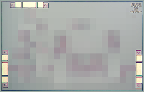
Port Diagram
A top-down view of the MDPX-00002CH package outline drawing is shown below.

Sales: 408-778-9952 | General: 408-778-4200 | Fax: 408-778-4300
Sales & Customer Support: [email protected]
Tech Support: [email protected]
The MDPX-00002CH is a broadband passive MMIC diplexer, a combination low pass and high pass filters, capable of multiplexing low pass DC - 35.0 GHz and high pass 43.3 - 59.9 GHz signals. Passive GaAs MMIC technology allows production of smaller filter constructions that replace larger form factor circuit board constructions. Tight fabrication tolerances allow for less unit-to-unit variation than traditional filter technologies. Low unit to unit variation allows for accurate simulations using the provided S3P file taken from measured production units.
N/A

| Part Number | Description | Package | Green Status | Product Lifecycle | Export Classification |
|---|---|---|---|---|---|
| MDPX-00002CH | Passive MMIC Diplexer | CH | RoHS REACH | Released | EAR99 |
| Part Number | Description | Package | Green Status | Product Lifecycle | Export Classification |
|---|---|---|---|---|---|
| MDPX-00002CH | Passive MMIC Diplexer | CH | RoHS REACH | Released | EAR99 |
MDPX-00002CH
Passive MMIC Diplexer
| Revision Code | Revision Date | Comment |
|---|---|---|
| - | 2023-08-30 | Datasheet Initial Release |
| A | 2024-01-05 | Updated Production Test Criteria |
| B | 2024-02-20 | Updated Package Dimension |
MDPX-00002CH
Passive MMIC Diplexer
A top-down view of the MDPX-00002CH package outline drawing is shown below.
| Port | Function | Description | DC Equivalent Circuit |
|---|---|---|---|
| GND | Ground | CH package ground path is provided through the substrate and ground bond pads. |  |
| Pad 1 | Input/common | Pad 1 is the common port. This pad is DC short to Pad 3 and DC open to Pad 2. |  |
| Pad 2 | RF High Band | Pad 2 is the high pass filter. This pad is DC open to ground and all other pads. |  |
| Pad 3 | RF Low Band | Pad 3 is the low pass filter. This pad is DC short Pad 1 and is DC open to Pad 2. | |
MDPX-00002CH
Passive MMIC Diplexer
The Absolute Maximum Ratings indicate limits beyond which damage may occur to the device. If these limits are exceeded, the device may be inoperable or have a reduced lifetime.
| Parameter | Maximum Rating | Unit |
|---|---|---|
| DC Current, at any Port | 500 | mA |
| Maximum Operating Temperature | 100 | °C |
| Maximum Storage Temperature | 125 | °C |
| Minimum Operating Temperature | -55 | °C |
| Minimum Storage Temperature | -65 | °C |
| Parameter | Details | Rating |
|---|---|---|
| Dimensions | - | 1.55 x 2.40 mm |
MDPX-00002CH
Passive MMIC Diplexer
The electrical specifications apply at TA=+25°C in a 50Ω system. Min and Max limits are guaranteed at TA=+25°C. All bare die are 100% visually inspected and RF performance is guaranteed by sample testing.
| Parameter | Test Conditions | Minimum Frequency (GHz) | Maximum Frequency (GHz) | Min | Typ | Max | Unit |
|---|---|---|---|---|---|---|---|
| 1 dBc High Passband | - | - | - | 43.3 | - | 59.9 | GHz |
| 1 dBc Low Passband | - | - | - | 0 | - | 35 | GHz |
| 3 dBc High Passband | - | - | - | 41.3 | - | 67 | GHz |
| 3 dBc Low Passband | - | - | - | 0 | - | 39.8 | GHz |
| Common Port Return Loss | - | 43.3 | 59.9 | - | 23 | - | dB |
| Common Port Return Loss | - | 0 | 35 | - | 22 | - | dB |
| Group Delay, High Band | - | 43.3 | 59.9 | - | 61 | - | ps |
| Group Delay, Low Band | - | 0 | 35 | - | 22 | - | ps |
| High Pass Filter, Pass Band Insertion Loss | - | 43.3 | 59.9 | - | 2 | - | dB |
| High Pass Filter, Pass Band Return Loss | - | 43.3 | 59.9 | - | 22 | - | dB |
| Impedance | - | - | - | - | 50 | - | Ω |
| Isolation | - | 43.3 | 67 | - | 41 | - | dB |
| Isolation | - | 0 | 38.1 | - | 44 | - | dB |
| Low Pass Filter, Pass Band Return Loss | - | 0 | 35 | - | 0 | - | dB |
| Low Pass Filter, Pass Band Return Loss | - | 0 | 35 | - | 21 | - | dB |
| Stopband Suppression, High Band | - | 0 | 38.1 | - | 46 | - | dB |
| Stopband Suppression, Low Band | - | 43.3 | 67 | - | 36 | - | dB |
MDPX-00002CH
Passive MMIC Diplexer


MDPX-00002CH
Passive MMIC Diplexer
Download : Outline 2D Drawing
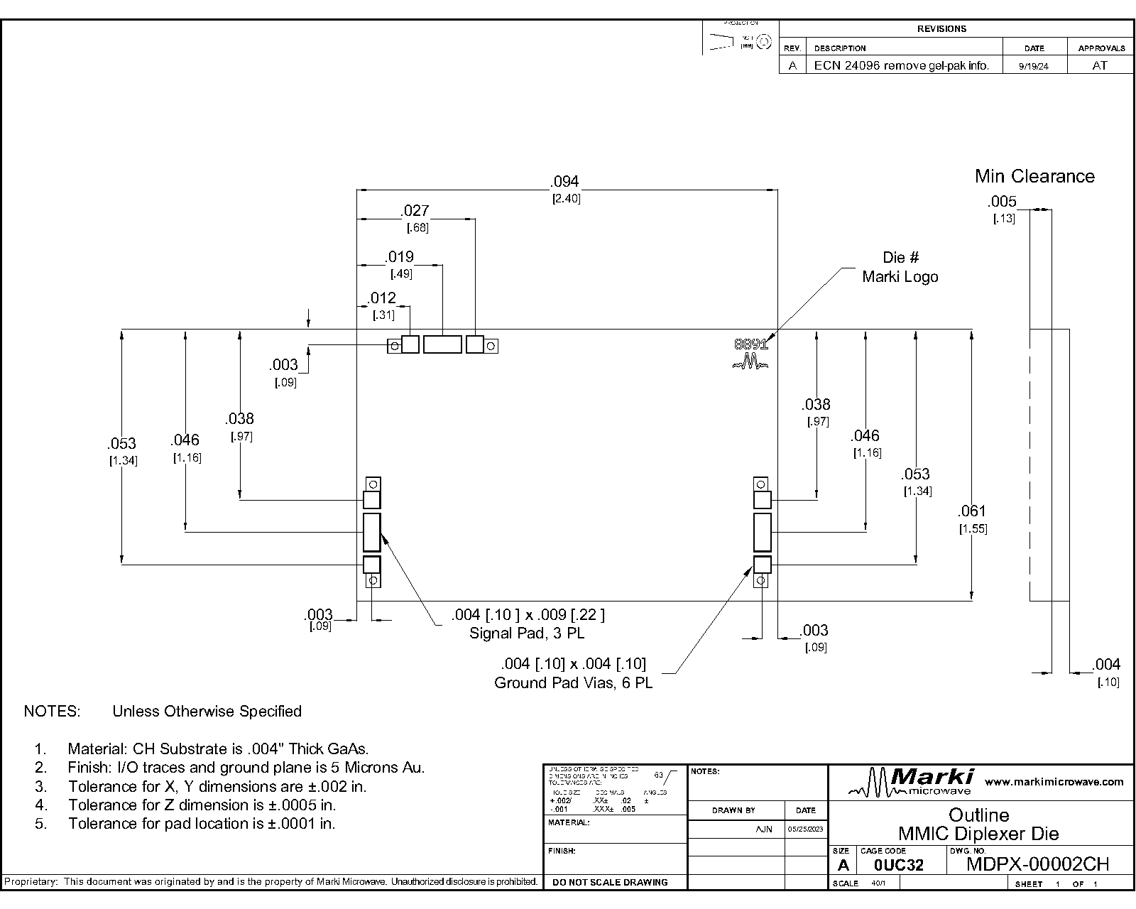
NOTES: Unless Otherwise Specified
1. Material: CH Substrate is .004" Thick GaAs.
2. Finish: I/O traces and ground plane is 5 Microns Au.
3. Tolerance for X, Y dimensions are ±.002 in.
4. Tolerance for Z dimension is ±.0005 in.
5. Tolerance for pad location is ±.0001 in.