Rev: A | Copyright © 2024 Marki Microwave LLC.

General Description

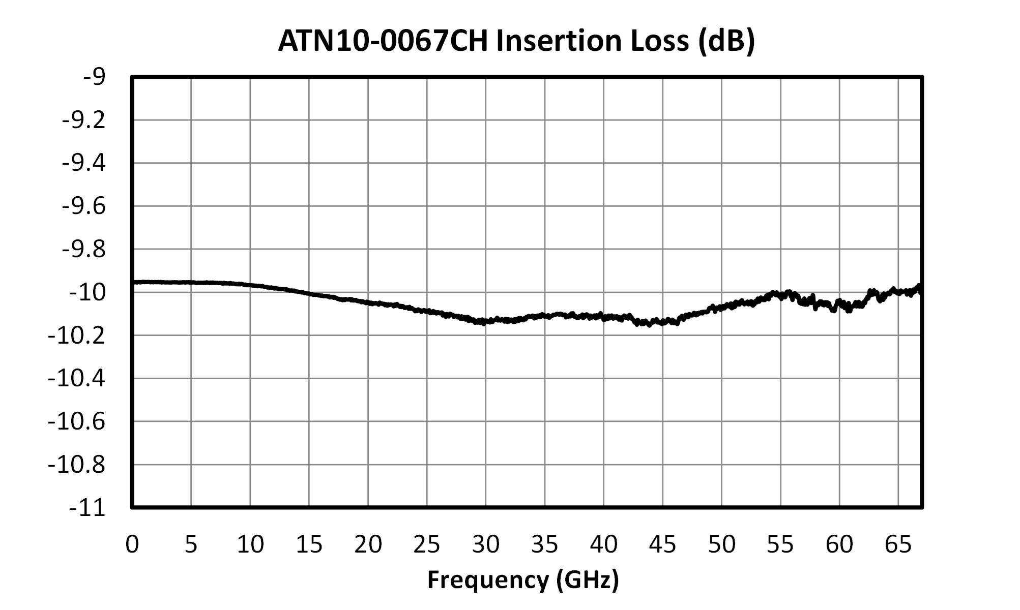
The ATN10-0067CH is part of a family of precision GaAs MMIC fixed attenuators. The ATN10-0067CH provides a nominal 10dB attenuation over a DC-67GHz operating range. These attenuators are an ideal solution for attenuating a signal and they can be used in a wide range of applications. They are ideal for test equipment’s protection and signal overload prevention in various RF systems. A 50-ohm match is maintained over the entire operating frequency range. ATN-67CH-KIT is an evaluation kit with 5 units of each value between 0dB to 10dB.

Features

  • 10dB attenuation
  • Additional attenuation values available between 0dB to 10dB in 1dB steps, 13dB, 15dB, 17dB, 20dB
  • Excellent Return Loss

Functional Block Diagram

Block Diagram
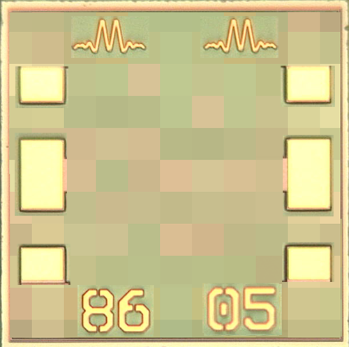
Photo of ATN10-0067CH

Electrical Performance Summary

ParameterTypUnit
Frequency Range0 to 67GHz
Attenuation 10dB
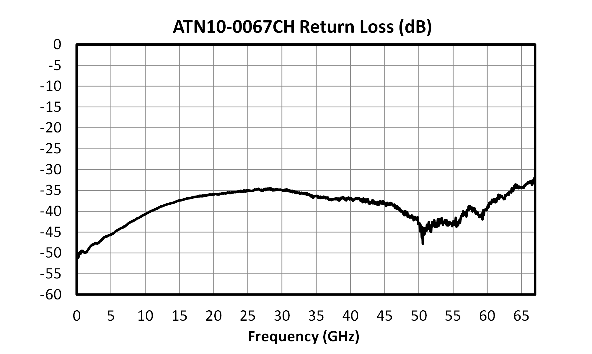
Return Loss 38dB
Attenuation Flatness 0.2dB

Summary only – refer to the Electrical Specifications, Absolute Maximum Ratings, and Recommended Operating Range tables for complete details.

Part Ordering Options

Part NumberDescriptionPackageGreen StatusProduct LifecycleExport Classification
ATN10-0067CHPassive GaAs MMIC DC - 67 GHz 10dB AttenuatorCH

RoHS

REACH

ReleasedEAR99

Table Of Contents

Typical Performance Plots

Insertion Loss vs Frequency graph for ATN10-0067CH
Return Loss vs Frequency graph for ATN10-0067CH

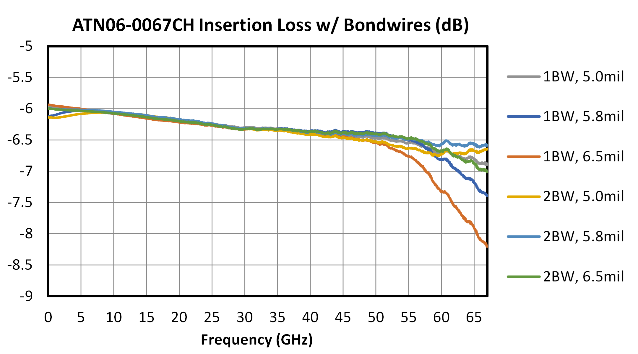
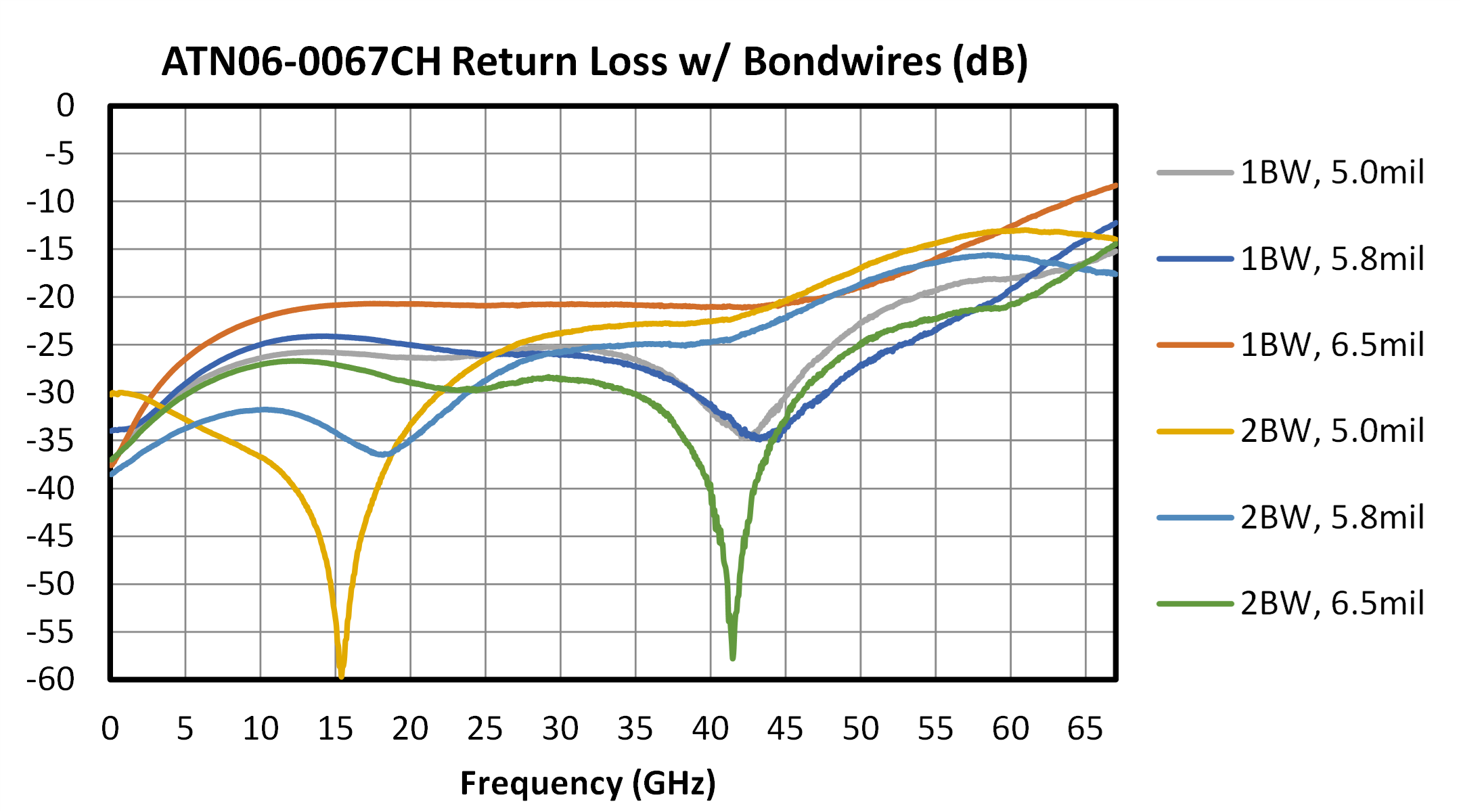
Variation With Bondwires

Typical variation with bondwire lengths is shown for ATN06-0067CH, however general trends withincreasing bondwire lengths apply to all attenuators in the family.

Insertion Loss with Bondwires (dB) graph for ATN10-0067CH
Return Loss with Bondwires (dB) graph for ATN10-0067CH

Specifications

Electrical Specifications

The electrical specifications apply at TA=+25°C in a 50Ω system. Min and Max limits are guaranteed at TA=+25°C. All bare die are 100% visually inspected and RF performance is guaranteed by sample testing.

ParameterTest ConditionsMinimum
Frequency
(GHz)
Maximum
Frequency
(GHz)
MinTypMaxUnit
Frequency Range-0 67---GHz
Attenuation -0 67-10-dB
Attenuation Flatness -0 67-0.2-dB
Impedance -0 67-50-Ω
Return Loss -0 35-36-dB
Return Loss -35 67-38-dB

Absolute Maximum Ratings

The Absolute Maximum Ratings indicate limits beyond which damage may occur to the device. If these limits are exceeded, the device may be inoperable or have a reduced lifetime.

ParameterMaximum RatingUnit
DC Current at any Port 100mA
Maximum Operating Temperature 100°C
Maximum Storage Temperature 125°C
Minimum Operating Temperature -55°C
Minimum Storage Temperature -65°C
RF Power Handling 2W

Package Information

ParameterDetailsRating
ESD250 to < 500 VoltsHBM Class 1A
Dimensions-0.60 x 0.60 mm

Port Configuration and Functions

Port Diagram

A top-down view of the ATN10-0067CH package outline drawing is shown below. The MMIC attenuators are symmetrical allowing Port 1 or Port 2 to be used as the input.

Diagram of the port configuration for ATN10-0067CH

Port Functions

PortFunctionDescriptionDC Equivalent
Circuit
PadGround CH package ground path is provided through the substrate and ground bond pads.Equivalent circuit for the Ground
Port 1Input/Output Port 1 and port 2 are DC connected to each other and ground through a T-network of resistors.Equivalent circuit for the Input/Output
Port 2Input/Output Port 1 and port 2 are DC connected to each other and ground through a T-network of resistors.Equivalent circuit for the Input/Output

Die Mounting Recommendations

Marki MMICs should be attached directly to a ground plane with conductive epoxy. The ground plane electrical impedance should be as low as practically possible. This will prevent resonances and permit the best possible electrical performance. Datasheet performance is only guaranteed in an environment with a low electrical impedance ground.

Mounting - To epoxy the chip, apply a minimum amount of conductive epoxy to the mounting surface so that a thin epoxy fillet is observed around the perimeter of the chip. Cure epoxy according to manufacturer instructions.

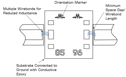
Wire Bonding - Ball or wedge bond with 0.025 mm (1 mil) diameter pure gold wire. Thermosonic wirebonding with a nominal stage temperature of 150 °C and a ball bonding force of 40 to 50 grams or wedge bonding force of 18 to 22 grams is recommended. Use the minimum level of ultrasonic energy to achieve reliable wirebonds. Wirebonds should be started on the chip and terminated on the package or substrate. Bond wire inductance will improve return loss. Bondwire inductance in the range of 30pH to 200pH will improve performance.

Circuit Considerations – 50 Ω transmission lines should be used for all high frequency connections in and out of the chip. Wirebonds should be kept as short as possible, with multiple wirebonds recommended for higher frequency connections to reduce parasitic inductance. In circumstances where the chip more than .001” thinner than the substrate, a heat spreading spacer tab is optional to further reduce bondwire length and parasitic inductance.

Bonding Diagram

Atnxx 0067 Ch Bonding Diagram

Handling Precautions


General Handling
Chips should be handled with care using tweezers or a vacuum collet. Users should take precautions to protect chips from direct human contact that can deposit contaminants, like perspiration and skin oils on any of the chip's surfaces.


Static Sensitivity
GaAs MMIC devices are sensitive to ESD and should be handled, assembled, tested, and transported only in static protected environments.


Cleaning and Storage: Do not attempt to clean the chip with a liquid cleaning system or expose the bare chips to liquid. Once the ESD sensitive bags the chips are stored in are opened, chips should be stored in a dry nitrogen atmosphere.

Mechanical Data

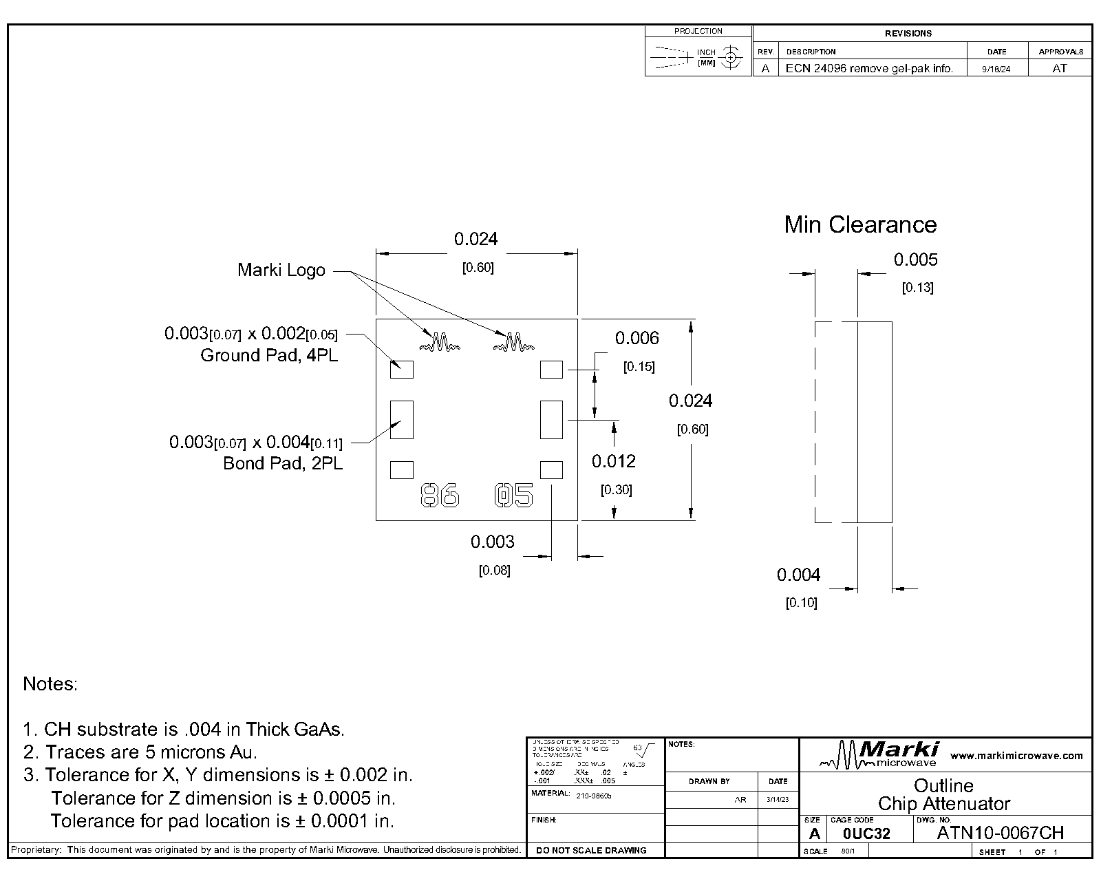
Outline Drawing

Download : Outline 2D Drawing

Outline Drawing

Revision History

Revision CodeRevision DateComment
A2024-01-05Updated Production Test Criteria

DISCLAIMER

MARKI MICROWAVE, LLC., (“MARKI”) PROVIDES TECHNICAL SPECIFICATIONS AND DATA (INCLUDING DATASHEETS), APPLICATION OR OTHER DESIGN ADVICE, WEB TOOLS, AND OTHER INFORMATION AND RESOURCES “AS IS” AND WITH ALL FAULTS. MARKI DISCLAIMS ALL WARRANTIES, EXPRESS OR IMPLIED, INCLUDING, WITHOUT LIMITATION, ANY IMPLIED WARRANTIES OF MERCHANTABILITY, FITNESS FOR A PARTICULAR PURPOSE, OR NON-INFRINGEMENT.

These resources are intended for developers skilled in the art designing with Marki products. You are solely responsible for (1) selecting the appropriate products for your application, (2) designing, validating, and testing your application, and (3) ensuring your application meets applicable standards and other requirements. Marki makes no guarantee regarding the suitability of its products for any particular purpose, nor does Marki assume any liability whatsoever arising out of your use or application of any Marki product.

Marki grants you permission to use these resources only for development of an application that uses Marki products. Other reproduction or use of these resources is strictly prohibited. No license is granted to any other Marki intellectual property or to any third-party intellectual property. Marki reserves the right to make changes to the product(s) or information contained herein without notice.

MARKI MICROWAVE, M wave logo, FastSwitch, and T3 MIXER are trademarks or registered trademarks of Marki Microwave, LLC. All other trademarks used are the property of their respective owners.

© 2024, Marki Microwave, LLC