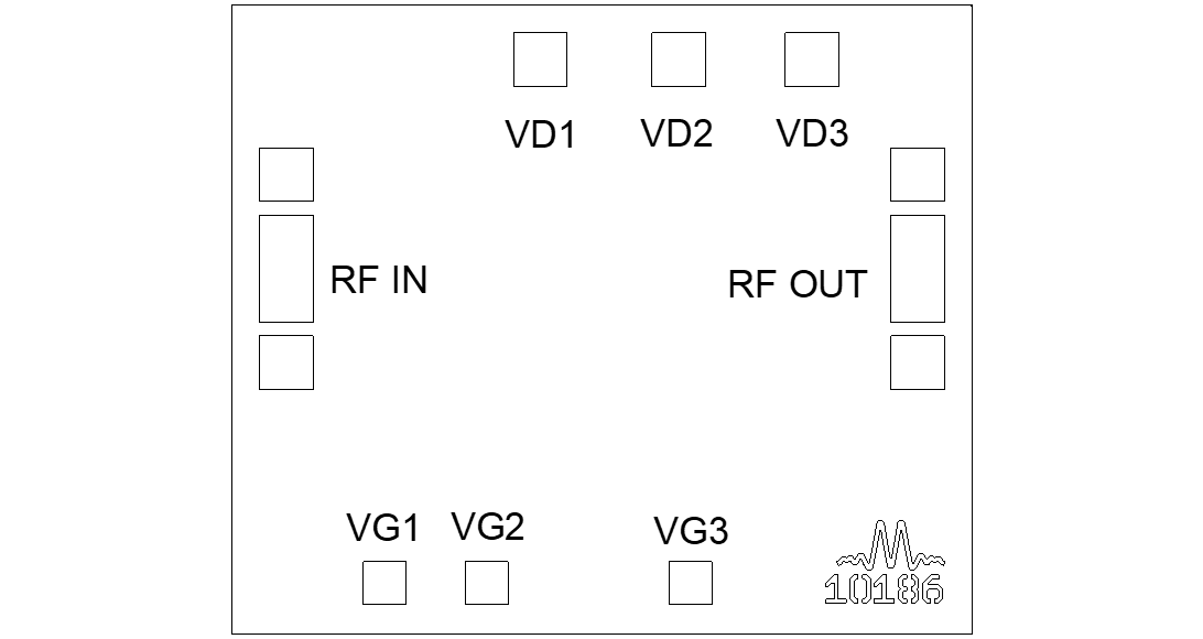
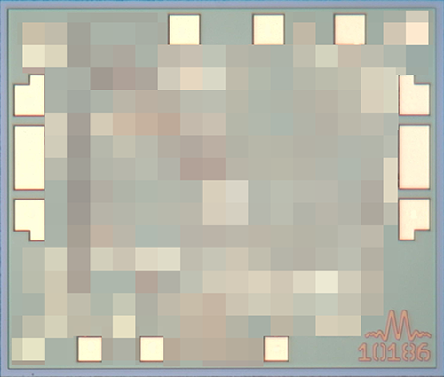
Port Diagram
A port diagram of the AMM-7199ACH is shown below.

Sales: 408-778-9952 | General: 408-778-4200 | Fax: 408-778-4300
Sales & Customer Support: [email protected]
Tech Support: [email protected]
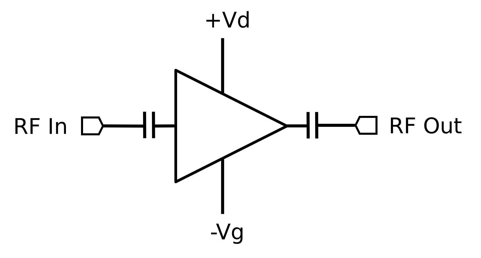
The AMM-7199 is a general-purpose broadband MMIC driver amplifier that provides +20 dBm output power suitable for driving a Marki H or L diode mixer at 11-38 GHz and S diode mixer from 15-32 GHz. The amplifier has excellent return losses, gain flatness and reduced current consumption. The small die size allows it to be used in a variety of applications and has built in DC-blocking capacitors on the input and output.
| Part Number | Description | Package | Green Status | Product Lifecycle | Export Classification |
|---|---|---|---|---|---|
| AMM-7199ACH | 11 GHz – 38 GHz GaAs Driver Amplifier | CH | REACH RoHS | Released | 3A001.b.2.d |
| Part Number | Description | Package | Green Status | Product Lifecycle | Export Classification |
|---|---|---|---|---|---|
| AMM-7199ACH | 11 GHz – 38 GHz GaAs Driver Amplifier | CH | REACH RoHS | Released | 3A001.b.2.d |
AMM-7199ACH
11 GHz – 38 GHz GaAs Driver Amplifier
| Revision Code | Revision Date | Comment |
|---|---|---|
| - | 2024-09-10 | Initial Release |
| A | 2025-04-02 | Outline Drawing update |
AMM-7199ACH
11 GHz – 38 GHz GaAs Driver Amplifier
A port diagram of the AMM-7199ACH is shown below.
AMM-7199ACH
11 GHz – 38 GHz GaAs Driver Amplifier
| Port | Function | Description | DC Equivalent Circuit |
|---|---|---|---|
| GND | Ground | Ground is provided through the backside of the die. The backside of the die must be connected to a DC/RF ground with high thermal and electrical conductivity. |  |
| RF In | RF Input | This is the RF Input port of the amplifier die. It is internally DC blocked and RF matched to 50 Ω. RF input pad is GSG with 175 µm pitch. | 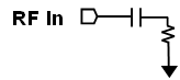 |
| RF Out | RF Output | This is the RF Output port of the amplifier die. It is internally DC blocked and RF matched to 50 Ω. RF output pad is GSG with 175 µm pitch. | 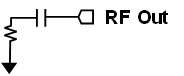 |
| VD1 | Drain Supply Voltage | Pad VD1 supplies the drain voltage to the first stage of the 3-stage amplifier IC. Apply gate voltage to VG pins before applying drain voltage. | 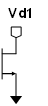 |
| VD2 | Drain Supply Voltage | Pad VD2 supplies the drain voltage to the first stage of the 3-stage amplifier IC. Apply gate voltage to VG pins before applying drain voltage. | 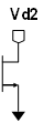 |
| VD3 | Drain Supply Voltage | Pad VD3 supplies the drain voltage to the first stage of the 3-stage amplifier IC. Apply gate voltage to VG pins before applying drain voltage. | 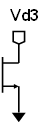 |
| VG1 | Gate Bias Voltage | VG1 provides the gate bias to the first stage of the 3-stage amplifier. The user should apply between -0.4 and -0.6V to VG1 pad before applying any VD drain supply. | 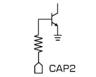 |
| VG2 | Gate Bias Voltage | VG2 provides the gate bias to the first stage of the 3-stage amplifier. The user should apply between -0.4 and -0.6V to VG2 pad before applying any VD drain supply. | |
| VG3 | Gate Bias Voltage | VG3 provides the gate bias to the first stage of the 3-stage amplifier. The user should apply between -0.4 and -0.6V to VG3 pad before applying any VD drain supply. | |
AMM-7199ACH
11 GHz – 38 GHz GaAs Driver Amplifier
The Absolute Maximum Ratings indicate limits beyond which damage may occur to the device. If these limits are exceeded, the device may become inoperable or have a reduced lifetime. This amplifier is designed and characterized in a 50Ω system, and operation in a reflective environment can cause performance degradation.
| Parameter | Maximum Rating | Unit |
|---|---|---|
| Continuous Power Dissipation (PDISS) (at 85 ˚C case temp.) 1 | 1 | W |
| Maximum Operating Temperature | 85 | °C |
| Maximum Storage Temperature | 150 | °C |
| Max Junction Temperature for MTTF > 1E6 Hours | 175 | °C |
| Minimum Operating Temperature | -40 | °C |
| Minimum Storage Temperature | -65 | °C |
| Negative Bias Voltage (Vg) | -2 | V |
| Positive Drain Supply Current (Id) (with RF Input) | 450 | mA |
| Positive Drain Supply Voltage (Vd) | 4.5 | V |
| RF Input Power | 20 | dBm |
| Thermal Resistance, θJC | 90 | ºC/W |
[1] Derates by 11 mW/ ˚C above 85 ˚C case temperature.
| Parameter | Details | Rating |
|---|---|---|
| Dimensions | - | 1.38x1.25 mm |
The Recommended Operating Conditions indicate the limits, inside which the device should be operated, to guarantee the performance given in Electrical Specifications Operating outside these limits may not necessarily cause damage to the device, but the performance may degrade outside the limits of the electrical specifications. For limits, above which damage may occur, see Absolute Maximum Ratings.
| Parameter | Min | Nominal | Max | Unit |
|---|---|---|---|---|
| Negative Bias Voltage (Vg) | -0.6 | -0.5 | -0.4 | V |
| Input Power for Saturation | 3 | 6 | 8 | dBm |
| Ambient Temperature | -40 | 25 | 85 | °C |
| Power Supply DC Voltage (Vd) | 2.5 | 3 | 3 | V |
| Power Supply DC Current (Id) (No RF Input) | 100 | 130 | 180 | mA |
AMM-7199ACH
11 GHz – 38 GHz GaAs Driver Amplifier
The electrical specifications apply at TA=+25°C in a 50Ω system. Min and Max limits apply only to our connectorized units and are guaranteed at TA=+25°C. Die are 100% DC tested and RF tested on a per lot basis.
| Parameter | Test Conditions | Minimum Frequency (GHz) | Maximum Frequency (GHz) | Min | Typ | Max | Unit |
|---|---|---|---|---|---|---|---|
| Current Consumption 1 | 3V/-0.4V | - | - | - | 180 | - | mA |
| Current Consumption 2 | 3V/-0.5V | - | - | - | 130 | - | mA |
| Current Consumption 3 | 3V/-0.6V | - | - | - | 100 | - | mA |
| Input Power for Saturation | 3V/-0.5V bias | 11 | 38 | - | 6 | - | dBm |
| Input Return Loss | 3V/-0.5V Bias | 11 | 38 | - | 18 | - | dB |
| Noise Figure | 3V/-0.5V bias | 11 | 38 | - | 5.5 | - | dB |
| Output IP3 | 3V/-0.5V, -20 dBm Input Power | 11 | 38 | - | 31 | - | dBm |
| Output P1dB | 3V/-0.5V bias | 11 | 38 | - | 18 | - | dBm |
| Output Return Loss | 3V/-0.5V Bias | 11 | 38 | - | 12 | - | dB |
| Reverse Isolation | 3V/-0.5V Bias | 11 | 38 | - | 60 | - | dB |
| Saturated Output Power 4 | 3V/-0.5V bias | 11 | 15 | - | 18 | - | dBm |
| Saturated Output Power 5 | 3V/-0.5V bias | 15 | 30 | 17 | 20 | - | dBm |
| Saturated Output Power 6 | 3V/-0.5V bias | 30 | 38 | - | 16 | - | dBm |
| Small Signal Gain | 3V/-0.5V bias | 15 | 30 | 17 | 20 | - | dB |
| Small Signal Gain | 3V/-0.5V bias | 11 | 15 | - | 18 | - | dB |
| Small Signal Gain | 3V/-0.5V bias | 30 | 38 | - | 14 | - | dB |
| Parameter | Test Conditions | Minimum Frequency (GHz) | Maximum Frequency (GHz) | Min | Typ | Max | Unit |
|---|---|---|---|---|---|---|---|
| Current Consumption 1 | 3V/-0.4V | - | - | - | 180 | - | mA |
| Current Consumption 2 | 3V/-0.5V | - | - | - | 130 | - | mA |
| Current Consumption 3 | 3V/-0.6V | - | - | - | 100 | - | mA |
| Input Power for Saturation | 3V/-0.5V bias | 11 | 38 | - | 6 | - | dBm |
| Input Return Loss | 3V/-0.5V Bias | 11 | 38 | - | 18 | - | dB |
| Noise Figure | 3V/-0.5V bias | 11 | 38 | - | 5.5 | - | dB |
| Output IP3 | 3V/-0.5V, -20 dBm Input Power | 11 | 38 | - | 31 | - | dBm |
| Output P1dB | 3V/-0.5V bias | 11 | 38 | - | 18 | - | dBm |
| Output Return Loss | 3V/-0.5V Bias | 11 | 38 | - | 12 | - | dB |
| Reverse Isolation | 3V/-0.5V Bias | 11 | 38 | - | 60 | - | dB |
| Saturated Output Power 4 | 3V/-0.5V bias | 11 | 15 | - | 18 | - | dBm |
| Saturated Output Power 5 | 3V/-0.5V bias | 15 | 30 | 17 | 20 | - | dBm |
| Saturated Output Power 6 | 3V/-0.5V bias | 30 | 38 | - | 16 | - | dBm |
| Small Signal Gain | 3V/-0.5V bias | 15 | 30 | 17 | 20 | - | dB |
| Small Signal Gain | 3V/-0.5V bias | 11 | 15 | - | 18 | - | dB |
| Small Signal Gain | 3V/-0.5V bias | 30 | 38 | - | 14 | - | dB |
[1][2][3] Bias conditions tested with no RF input power. Bias conditions presented as Vd/Vg.
[4][5][6] Saturated Output Power specification defined using the AMM-7199UC.
AMM-7199ACH
11 GHz – 38 GHz GaAs Driver Amplifier
%20vs.%20Frequency,%20over%20Bias.png)
%20vs.%20Frequency,%20over%20Bias.png)
%20vs.%20Frequency,%20over%20Bias.png)
%20vs.%20Frequency,%20over%20Bias.png)
%20vs.%20Frequency,%20over%20Bias.png)
%20vs.%20Frequency,%20over%20Bias.png)
%20vs.%20Frequency,%20over%20Bias.png)
%20vs.%20Frequency%20at%20Vd%20=%203V,%20Idq%20=%2091mA.png)
AMM-7199ACH
11 GHz – 38 GHz GaAs Driver Amplifier
%20vs.%20Frequency%20at%20Vd%20=%203V,%20Idq%20=%20130mA.png)
%20vs.%20Frequency%20at%20Vd%20=%203V,%20Idq%20=%20175mA.png)
AMM-7199ACH
11 GHz – 38 GHz GaAs Driver Amplifier
AMM-7199ACH
11 GHz – 38 GHz GaAs Driver Amplifier
Download : Outline 2D Drawing
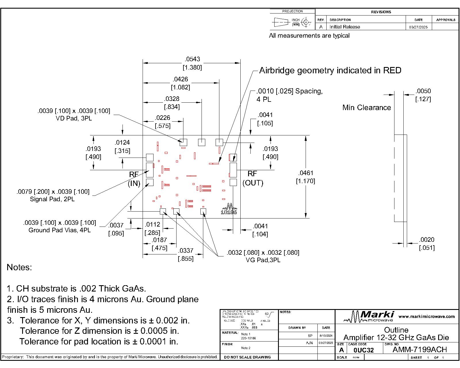
Notes:
1. CH substrate is .002 Thick GaAs.
2. I/O traces finish is 4 microns Au. Ground plane finish is 5 microns Au.
3. Tolerance for X, Y dimensions is ± 0.002 in.
Tolerance for Z dimension is ± 0.0005 in.
Tolerance for pad location is ± 0.0001 in.
AMM-7199ACH
11 GHz – 38 GHz GaAs Driver Amplifier