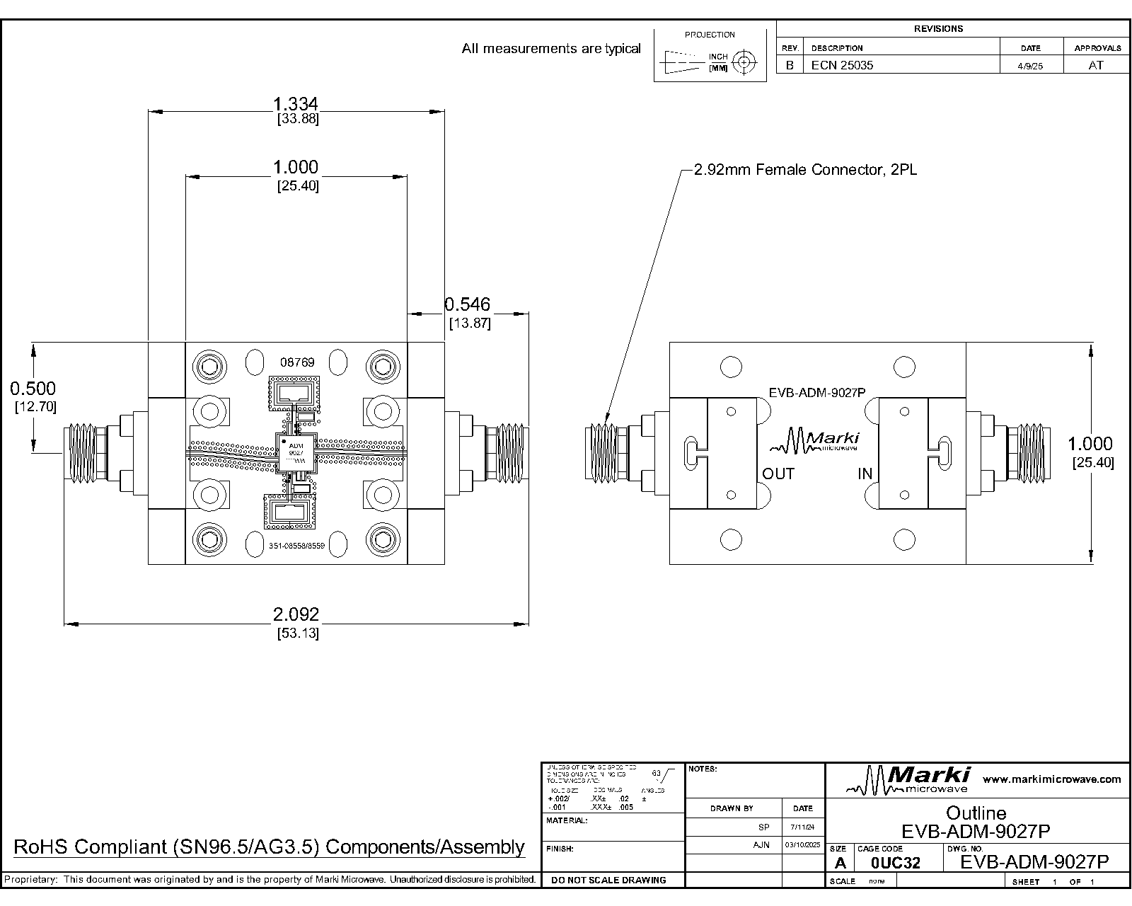
Port Diagram
A port diagram of the ADM-9027CH is shown below.

Sales: 408-778-9952 | General: 408-778-4200 | Fax: 408-778-4300
Sales & Customer Support: [email protected]
Tech Support: [email protected]
The ADM-9027CH is a wideband distributed low noise amplifier capable of providing 16 dB gain and +25 dBm OIP3 from 2 to 20 GHz and a low 2.5 dB typical noise figure from 7 to 18 GHz. The ADM-9027CH is an ideal linear signal amplifier for applications requiring low power consumption and small form-factors. The amplifier has excellent return losses and gain flatness and includes integrated DC blocking capacitors and RF choke.

| Part Number | Description | Package | Green Status | Product Lifecycle | Export Classification |
|---|---|---|---|---|---|
| ADM-9027CH | 2-24 GHz Distributed Amplifier | CH | RoHS | Released | EAR99 |
| Part Number | Description | Package | Green Status | Product Lifecycle | Export Classification |
|---|---|---|---|---|---|
| ADM-9027CH | 2-24 GHz Distributed Amplifier | CH | RoHS | Released | EAR99 |
ADM-9027CH
2-24 GHz Distributed Amplifier
| Revision Code | Revision Date | Comment |
|---|---|---|
| - | 2024-04-08 | Datasheet Initial Release |
ADM-9027CH
2-24 GHz Distributed Amplifier
A port diagram of the ADM-9027CH is shown below.
ADM-9027CH
2-24 GHz Distributed Amplifier
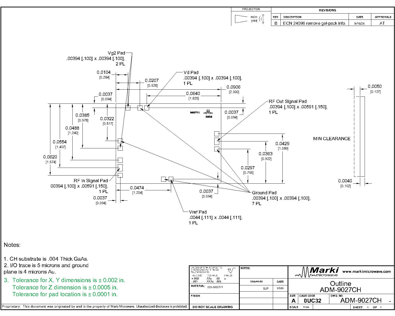
| Port | Function | Description | DC Equivalent Circuit |
|---|---|---|---|
| GND | Ground | DC and RF Ground is provided through the backside of the die. |  |
| NC | Non-connect (NC) | Do not connect to or ground these pads. Leave them floating for normal operation. | - |
| RF In | RF Input | This is the amplifiers RF input port. It is internally matched to 50 Ohms and is internally DC blocked. |  |
| RF Out | RF Output | This is the amplifiers RF output port. This port is internally matched to 50 Ohms and is internally DC blocked. | |
| Vb | Positive Bias Pin | This is the positive DC bias voltage for the amplifier IC. The voltage at this pin controls the current draw Id of the part. Higher voltage results in higher current. For normal operation, the voltage at this pin is adjusted to produce an Id of 60mA when Vd=6V. Alternatively, it is possible to use a single positive voltage supply and a 751Ohm resistor between Vd and Vb pins. This part requires off-chip bypass capacitors of 100pF and 0.1uF installed at this pin as close to the IC as possible. See applications circuit. |  |
| Vd | Positive DC Supply Voltage | This is the positive DC supply voltage for the amplifier IC. This pin is nominally set to +6V. This part requires off-chip bypass capacitors of 100pF and 0.1uF installed at this pin as close to the IC as possible. See applications circuit. |  |
ADM-9027CH
2-24 GHz Distributed Amplifier
The Absolute Maximum Ratings indicate limits beyond which damage may occur to the device. If any one of these limits are exceeded, the device may become inoperable or have a reduced lifetime. Reliability limits are individual, instantaneous catastrophic limits only. Functional operation limits are indicated below. Operation of the device at multiple absolute maximum limits or for extended periods at a single limit can cause degradation and damage to the device.
| Parameter | Maximum Rating | Unit |
|---|---|---|
| Bias Supply Voltage (Vb) | 6.5 | V |
| Drain Current (Id) (No RF Applied) | 85 | mA |
| Maximum Operating Temperature for MTTF > 1E6 hours | 85 | °C |
| Maximum Storage Temperature | 125 | °C |
| Minimum Operating Temperature for MTTF > 1E6 hours | -40 | °C |
| Minimum Storage Temperature | -65 | °C |
| Positive Drain Supply Voltage (Vd) | 8 | V |
| RF Input Power | 15 | dBm |
| Parameter | Details | Rating |
|---|---|---|
| Dimensions | - | 2.3 x 1.75mm |
The Recommended Operating Conditions indicate the limits, inside which the device should be operated, to guarantee the performance given in Electrical Specifications Operating outside these limits may not necessarily cause damage to the device, but the performance may degrade outside the limits of the electrical specifications. For limits, above which damage may occur, see Absolute Maximum Ratings.
| Parameter | Min | Nominal | Max | Unit |
|---|---|---|---|---|
| Positive DC Voltage (Vd) | 5 | 6 | 7 | V |
| Positive DC Bias Voltage (Vb) | 2 | 2.3 | 3 | V |
| Positive DC Current (Id) (No RF Input) | 50 | 60 | 77 | mA |
| Ambient Temperature | -40 | 25 | 85 | °C |
ADM-9027CH
2-24 GHz Distributed Amplifier
Unless otherwise specified, electrical specifications apply at TA=+25°C, Vd = 6V and Vb set such that Id=60mA.
| Parameter | Test Conditions | Minimum Frequency (GHz) | Maximum Frequency (GHz) | Min | Typ | Max | Unit |
|---|---|---|---|---|---|---|---|
| Input Return Loss | Vd=6V, Id=60mA | 2 | 24 | - | 15 | - | dB |
| Noise Figure | Vd=6V, Id=60mA | 7 | 18 | - | 2.5 | - | dB |
| Noise Figure | Vd=6V, Id=60mA | 18 | 24 | - | 3.5 | - | dB |
| Noise Figure | Vd=6V, Id=60mA | 2 | 7 | - | 3.5 | - | dB |
| Output IP3 | Vd=6V, Id=60mA | 2 | 20 | - | 25 | - | dBm |
| Output IP3 | Vd=6V, Id=60mA | 20 | 24 | - | 22 | - | dBm |
| Output P1dB | Vd=6V, Id=60mA | 2 | 12 | - | 16 | - | dBm |
| Output P1dB | Vd=6V, Id=60mA | 12 | 24 | - | 13 | - | dBm |
| Output Return Loss | Vd=6V, Id=60mA | 2 | 24 | - | 15 | - | dB |
| Reverse Isolation | Vd=6V, Id=60mA | 2 | 24 | - | 40 | - | dB |
| Small Signal Gain | Vd=6V, Id=60mA | 2 | 24 | 14 | 16 | - | dB |
ADM-9027CH
2-24 GHz Distributed Amplifier


ADM-9027CH
2-24 GHz Distributed Amplifier

ADM-9027CH
2-24 GHz Distributed Amplifier
Download : Outline 2D Drawing
Notes:
ADM-9027CH
2-24 GHz Distributed Amplifier