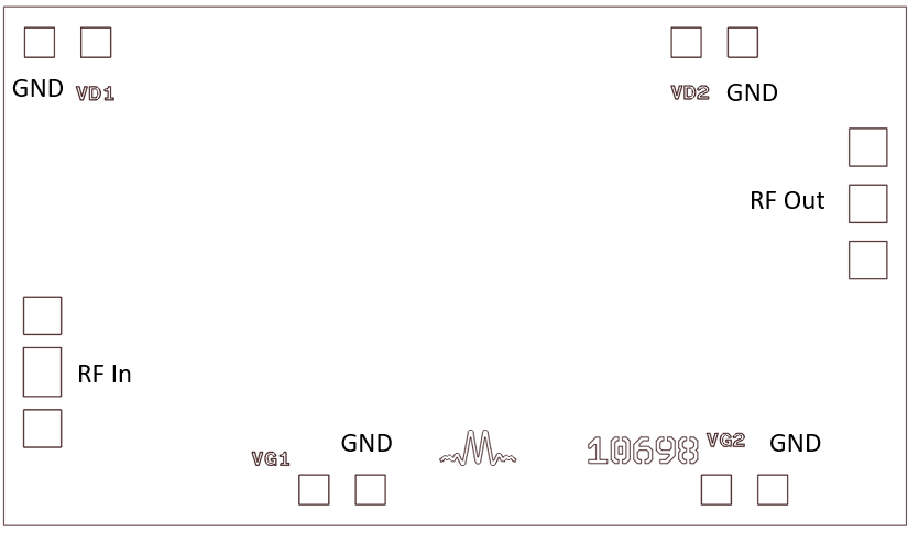
Port Diagram
A port diagram of the ADM-8007CH is shown below. The pad functions are detailed in this datasheet.
Sales: 408-778-9952 | General: 408-778-4200 | Fax: 408-778-4300
Sales & Customer Support: [email protected]
Tech Support: [email protected]
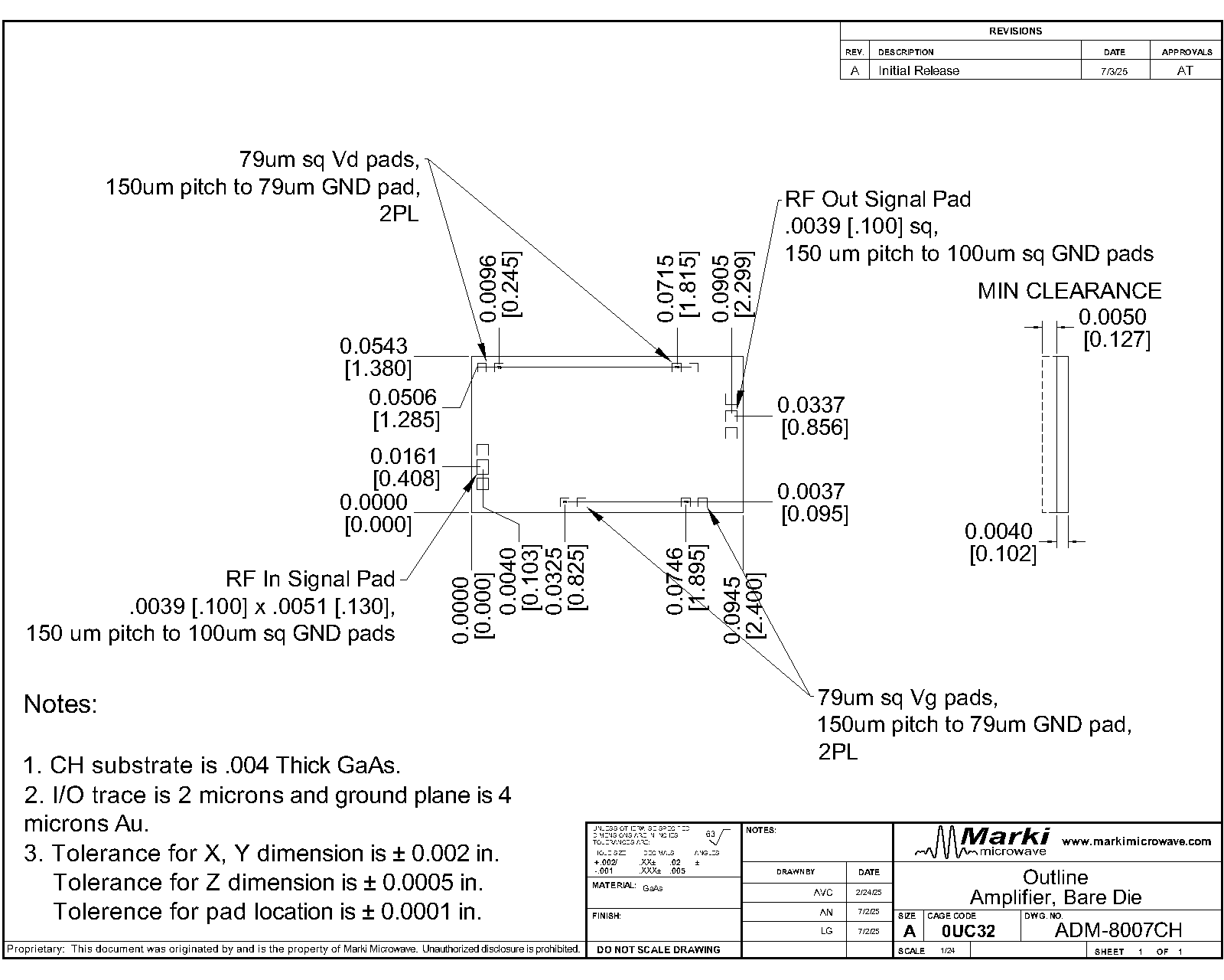
The ADM-8007CH is a high-linearity, high gain, low noise distributed amplifier capable of providing 23 dB gain, +23 dBm output power and 30 dBm OIP3 over a 2 to 40 GHz band. When driven with an input power of 0 to +5 dBm, the ADM-8007CH can provide sufficient LO drive to power all H and most S diode mixers to 40GHz. The amplifier requires a positive-only bias with no sequencing and has excellent return losses and gain flatness.

| Part Number | Description | Package | Green Status | Product Lifecycle | Export Classification |
|---|---|---|---|---|---|
| ADM-8007CH | 2 - 40 GHz High Gain Distributed Amplifier, Bare Die | CH | REACH RoHS | Released | 3A001.b.2.d |
| ADM-8007KGD | Known Good Die, 2 - 40 GHz High Gain Distributed Amplifier, Bare Die | CH | REACH RoHS | Released | 3A001.b.2.d |
ADM-8007CH
2 - 40 GHz High Gain Distributed Amplifier, Bare Die
| Revision Code | Revision Date | Comment |
|---|---|---|
| - | 2025-10-14 | Initial Release |
ADM-8007CH
2 - 40 GHz High Gain Distributed Amplifier, Bare Die
A port diagram of the ADM-8007CH is shown below. The pad functions are detailed in this datasheet.
ADM-8007CH
2 - 40 GHz High Gain Distributed Amplifier, Bare Die
| Port | Function | Description | DC Equivalent Circuit |
|---|---|---|---|
| GND | Ground | DC and RF Ground is provided through the backside of the die. | - |
| RF In | RF Input | RF In is the amplifier RF input. This pin is internally DC blocked and RF matched to 50 Ohms. | - |
| RF Out | RF Output | RF Out is the amplifier RF output. This pin is internally DC blocked and RF matched to 50 Ohms. | - |
| Vd1 | Drain Supply Pad | Vd1 is the DC supply pin for the amplifier’s input stage. | - |
| Vd2 | Drain Supply Pad | Vd2 is the DC supply pin for the amplifier’s output stage. | - |
| Vg1 | Gate Bias Voltage Pad | Vg1 provides bias for an internal current mirror that sets the current draw for amplifier input stage. Increasing current will increase gain at the expense of efficiency. | - |
| Vg2 | Gate Bias Voltage Pad | Vg2 provides bias for an internal current mirror that sets the current draw for amplifier output stage. Increasing current will increase gain at the expense of efficiency. | - |
ADM-8007CH
2 - 40 GHz High Gain Distributed Amplifier, Bare Die
The Absolute Maximum Ratings indicate limits beyond which damage may occur to the device. If any one of these limits are exceeded, the device may become inoperable or have a reduced lifetime. Reliability limits are individual, instantaneous catastrophic limits only. Functional operation limits are indicated below. Operation of the device at multiple absolute maximum limits or for extended periods at a single limit can cause degradation and damage to the device.
| Parameter | Maximum Rating | Unit |
|---|---|---|
| Bias Current (Ig1) | 45 | mA |
| Bias Current (Ig2) | 45 | mA |
| Bias Voltage (Vg1) | 5 | V |
| Bias Voltage (Vg2) | 5 | V |
| Drain Current (Id1) | 133 | mA |
| Drain Current (Id2) | 266 | mA |
| Drain Supply Voltage (Vd1) | 8 | V |
| Drain Supply Voltage (Vd2) | 8 | V |
| Maximum Operating Temperature for MTTF > 1E6 hours | 125 | °C |
| Maximum Storage Temperature | 150 | °C |
| Max Junction Temperature for MTTF of 1E6 hours | 175 | °C |
| Max Power Dissipation for MTTF of 1E6 hours | 1.6 | W |
| Minimum Operating Temperature for MTTF > 1E6 hours | -40 | °C |
| Minimum Storage Temperature | -65 | °C |
| RF Input Power | 15 | dBm |
| θ_Jc, Junction to Case Thermal Resistance | 30 | ºC/W |
| Parameter | Details | Rating |
|---|---|---|
| ESD | 50 to < 125 Volts | HBM 0A |
The Recommended Operating Conditions indicate the limits, inside which the device should be operated, to guarantee the performance given in Electrical Specifications Operating outside these limits may not necessarily cause damage to the device, but the performance may degrade outside the limits of the electrical specifications. For limits, above which damage may occur, see Absolute Maximum Ratings.
| Parameter | Min | Nominal | Max | Unit |
|---|---|---|---|---|
| Power Supply Voltage (Vg2) | - | 4 | 5 | V |
| Power Supply DC Current (Ig2) (No RF Input) 1 | - | 11 | 14 | mA |
| Power Supply DC Current (Id2) (No RF Input) 2 | - | 185 | 250 | mA |
| Power Supply DC Voltage (Vd2) | - | 4 | 5 | V |
| Power Supply DC Current (Ig1) (No RF Input) 3 | - | 9 | 11 | mA |
| Power Supply DC Voltage (Vd1) | - | 5 | 6 | V |
| Power Supply DC Current (Id1) (No RF Input) 4 | - | 50 | 83 | mA |
| Power Supply Voltage (Vg1) | - | 2.5 | 3.5 | V |
| Input Power for Saturation | 0 | 1 | 8 | dBm |
| Ambient Temperature | -40 | 25 | 85 | °C |
[1][3] Recommended operating current conditions without RF input applied. Bias current into Vg pin.
[2][4] Recommended operating current conditions without RF input applied. Bias current into Vd pin.
ADM-8007CH
2 - 40 GHz High Gain Distributed Amplifier, Bare Die
Unless otherwise specified, electrical specifications apply at TA=+25°C, Vd1,Vd2= 5 V, Vg1=3.5V, Vg2=4V. Min and Max limits apply only to our connectorized units and are guaranteed at TA=+25°C
| Parameter | Test Conditions | Minimum Frequency (GHz) | Maximum Frequency (GHz) | Min | Typ | Max | Unit |
|---|---|---|---|---|---|---|---|
| Current Consumption | Vd1, Vd2 = 5V,
Vg1= 3.5V, Vg2= 4V
no RF input | - | - | - | 237 | - | mA |
| Input IP3 | Vd1, Vd2 = 5V,
Vg1= 3.5V, Vg2= 4V
Pin = -15 dBm per tone, 10 MHz tone spacing | 2 | 27 | - | 11 | - | dBm |
| Input IP3 | Vd1, Vd2, Vg1, Vg2 = 5 V Pin = -15 dBm per tone, 10 MHz tone spacing | 27 | 40 | - | 6 | - | dBm |
| Input Power for Saturation | Vd1, Vd2 = 5V,
Vg1= 3.5V, Vg2= 4V | 27 | 40 | - | 0 | - | dBm |
| Input Power for Saturation | Vd1, Vd2 = 5V,
Vg1= 3.5V, Vg2= 4V | 2 | 27 | - | 2 | - | dBm |
| Input Return Loss | Vd1, Vd2, Vg1, Vg2 = 5 V Pin = -20 dBm | 2 | 40 | - | 20 | - | dB |
| Noise Figure | Vd1, Vd2 = 5V,
Vg1= 3.5V, Vg2= 4V
Pin = -20 dBm | 8 | 27 | - | 3 | - | dB |
| Noise Figure | Vd1, Vd2 = 5V,
Vg1= 3.5V, Vg2= 4V
Pin = -20 dBm | 27 | 40 | - | 4.2 | - | dB |
| Noise Figure | Vd1, Vd2 = 5V,
Vg1= 3.5V, Vg2= 4V
Pin = -20 dBm | 2 | 8 | - | 5 | - | dB |
| Output IP2 | Vd1, Vd2 = 5V,
Vg1= 3.5V, Vg2= 4V
Pin = -15 dBm per tone, 10 MHz tone spacing | 12 | 20 | - | 45 | - | dBm |
| Output IP2 | Vd1, Vd2 = 5V,
Vg1= 3.5V, Vg2= 4V
Pin = -15 dBm per tone, 10 MHz tone spacing | 2 | 12 | - | 49 | - | dBm |
| Output IP3 | Vd1, Vd2 = 5V,
Vg1= 3.5V, Vg2= 4V
Pin = -15 dBm per tone, 10 MHz tone spacing | 2 | 27 | - | 33 | - | dBm |
| Output IP3 | Vd1, Vd2 = 5V,
Vg1= 3.5V, Vg2= 4V
Pin = -15 dBm per tone, 10 MHz tone spacing | 27 | 40 | - | 25 | - | dBm |
| Output P1dB | Vd1, Vd2 = 5V,
Vg1= 3.5V, Vg2= 4V | 27 | 40 | - | 19 | - | dBm |
| Output P1dB | Vd1, Vd2 = 5V,
Vg1= 3.5V, Vg2= 4V | 2 | 27 | - | 21 | - | dBm |
| Output Return Loss | Vd1, Vd2 = 5V,
Vg1= 3.5V, Vg2= 4V
Pin = -20 dBm | 2 | 40 | - | 22 | - | dB |
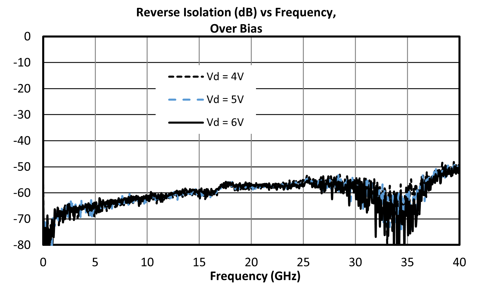
| Reverse Isolation | Vd1, Vd2 = 5V,
Vg1= 3.5V, Vg2= 4V
Pin = -20 dBm | 2 | 40 | - | 60 | - | dB |
| Saturated Output Power | Vd1, Vd2 = 5V,
Vg1= 3.5V, Vg2= 4V | 27 | 40 | - | 21 | - | dBm |
| Saturated Output Power | Vd1, Vd2 = 5V, Vg1 = 3.5V, Vg2 = 4V | 2 | 27 | - | 23 | - | dBm |
| Small Signal Gain | Vd1, Vd2 = 5V,
Vg1= 3.5V, Vg2= 4V
Pin = -20 dBm | 2 | 40 | - | 23 | - | dB |
| Parameter | Test Conditions | Minimum Frequency (GHz) | Maximum Frequency (GHz) | Min | Typ | Max | Unit |
|---|---|---|---|---|---|---|---|
| Current Consumption | Vd1, Vd2 = 5V,
Vg1= 3.5V, Vg2= 4V
no RF input | - | - | - | 237 | - | mA |
| Input IP3 | Vd1, Vd2 = 5V,
Vg1= 3.5V, Vg2= 4V
Pin = -15 dBm per tone, 10 MHz tone spacing | 2 | 27 | - | 11 | - | dBm |
| Input IP3 | Vd1, Vd2, Vg1, Vg2 = 5 V Pin = -15 dBm per tone, 10 MHz tone spacing | 27 | 40 | - | 6 | - | dBm |
| Input Power for Saturation | Vd1, Vd2 = 5V,
Vg1= 3.5V, Vg2= 4V | 27 | 40 | - | 0 | - | dBm |
| Input Power for Saturation | Vd1, Vd2 = 5V,
Vg1= 3.5V, Vg2= 4V | 2 | 27 | - | 2 | - | dBm |
| Input Return Loss | Vd1, Vd2, Vg1, Vg2 = 5 V Pin = -20 dBm | 2 | 40 | - | 20 | - | dB |
| Noise Figure | Vd1, Vd2 = 5V,
Vg1= 3.5V, Vg2= 4V
Pin = -20 dBm | 8 | 27 | - | 3 | - | dB |
| Noise Figure | Vd1, Vd2 = 5V,
Vg1= 3.5V, Vg2= 4V
Pin = -20 dBm | 27 | 40 | - | 4.2 | - | dB |
| Noise Figure | Vd1, Vd2 = 5V,
Vg1= 3.5V, Vg2= 4V
Pin = -20 dBm | 2 | 8 | - | 5 | - | dB |
| Output IP2 | Vd1, Vd2 = 5V,
Vg1= 3.5V, Vg2= 4V
Pin = -15 dBm per tone, 10 MHz tone spacing | 12 | 20 | - | 45 | - | dBm |
| Output IP2 | Vd1, Vd2 = 5V,
Vg1= 3.5V, Vg2= 4V
Pin = -15 dBm per tone, 10 MHz tone spacing | 2 | 12 | - | 49 | - | dBm |
| Output IP3 | Vd1, Vd2 = 5V,
Vg1= 3.5V, Vg2= 4V
Pin = -15 dBm per tone, 10 MHz tone spacing | 2 | 27 | - | 33 | - | dBm |
| Output IP3 | Vd1, Vd2 = 5V,
Vg1= 3.5V, Vg2= 4V
Pin = -15 dBm per tone, 10 MHz tone spacing | 27 | 40 | - | 25 | - | dBm |
| Output P1dB | Vd1, Vd2 = 5V,
Vg1= 3.5V, Vg2= 4V | 27 | 40 | - | 19 | - | dBm |
| Output P1dB | Vd1, Vd2 = 5V,
Vg1= 3.5V, Vg2= 4V | 2 | 27 | - | 21 | - | dBm |
| Output Return Loss | Vd1, Vd2 = 5V,
Vg1= 3.5V, Vg2= 4V
Pin = -20 dBm | 2 | 40 | - | 22 | - | dB |
| Reverse Isolation | Vd1, Vd2 = 5V,
Vg1= 3.5V, Vg2= 4V
Pin = -20 dBm | 2 | 40 | - | 60 | - | dB |
| Saturated Output Power | Vd1, Vd2 = 5V,
Vg1= 3.5V, Vg2= 4V | 27 | 40 | - | 21 | - | dBm |
| Saturated Output Power | Vd1, Vd2 = 5V, Vg1 = 3.5V, Vg2 = 4V | 2 | 27 | - | 23 | - | dBm |
| Small Signal Gain | Vd1, Vd2 = 5V,
Vg1= 3.5V, Vg2= 4V
Pin = -20 dBm | 2 | 40 | - | 23 | - | dB |
ADM-8007CH
2 - 40 GHz High Gain Distributed Amplifier, Bare Die
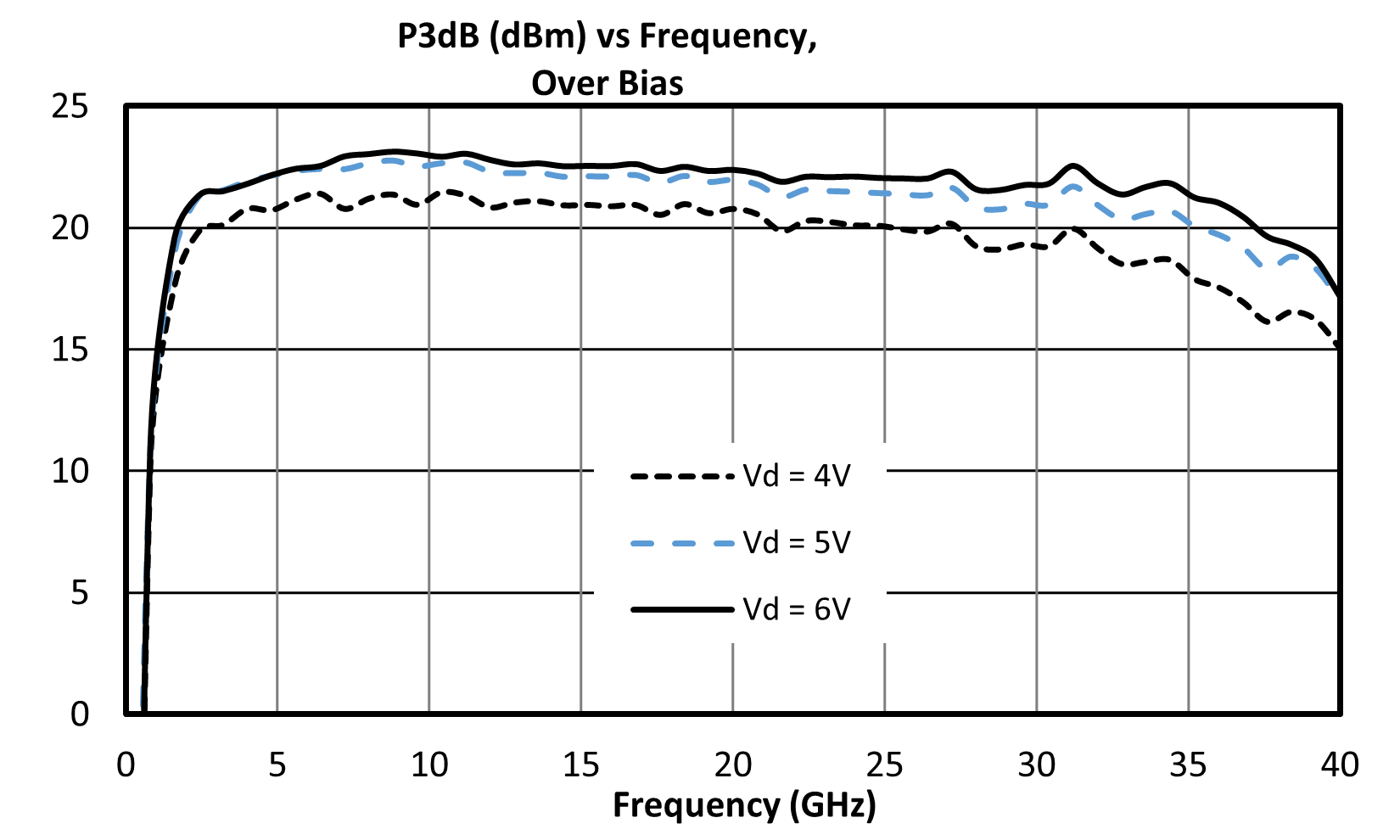
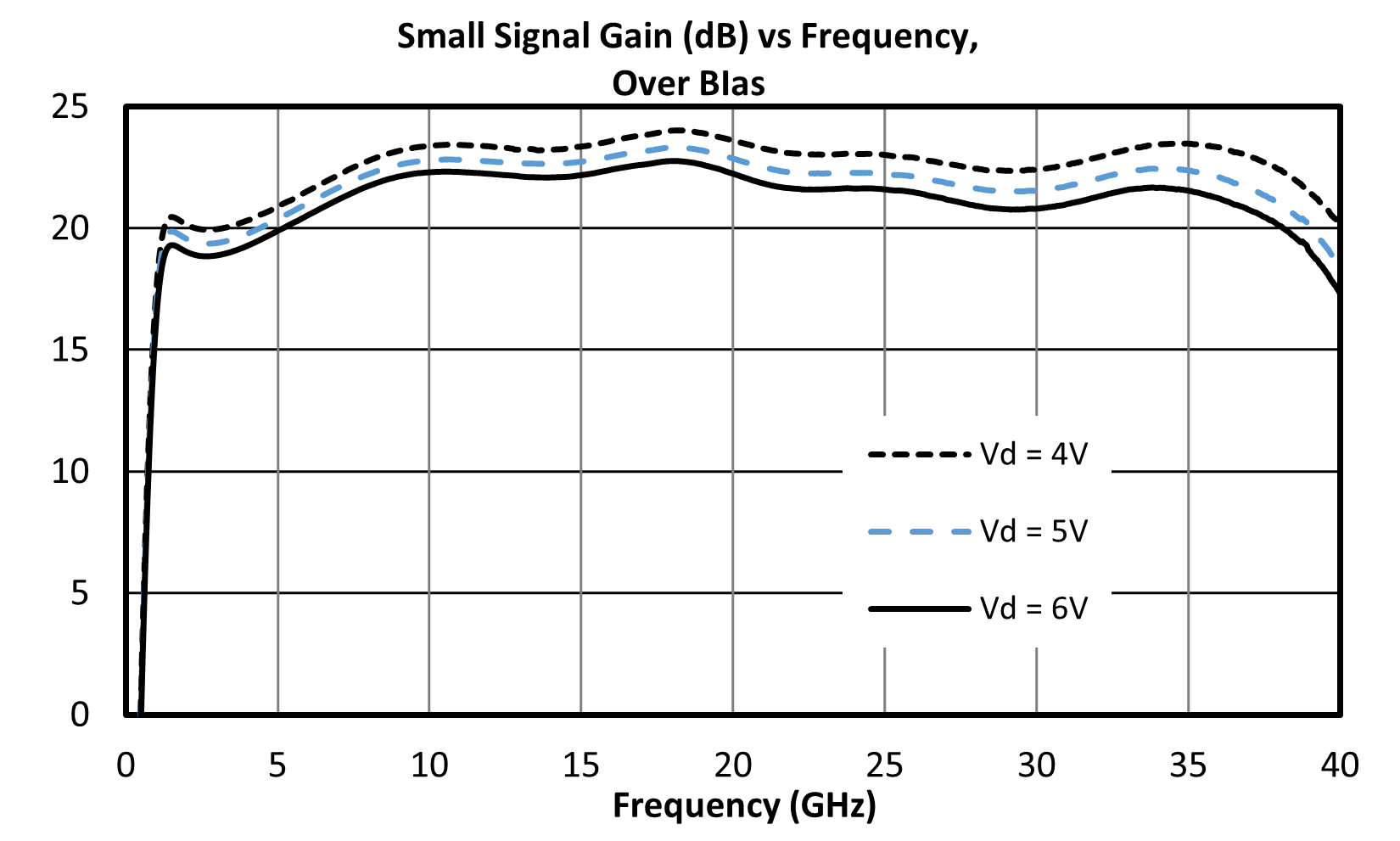
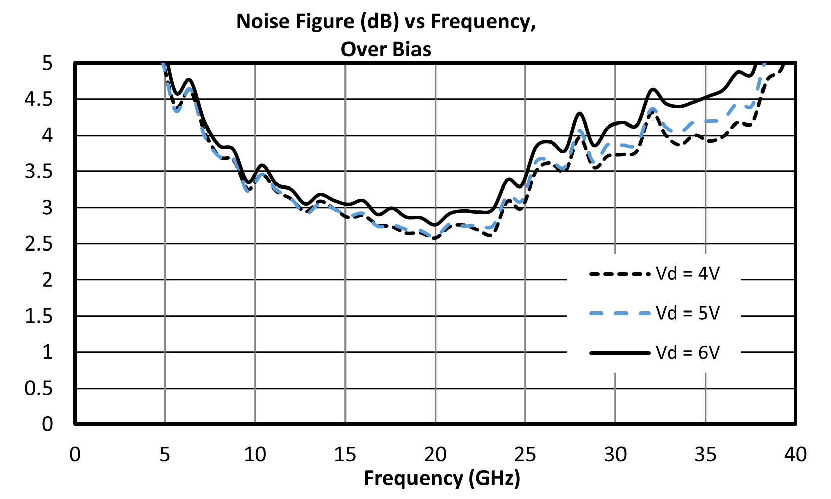
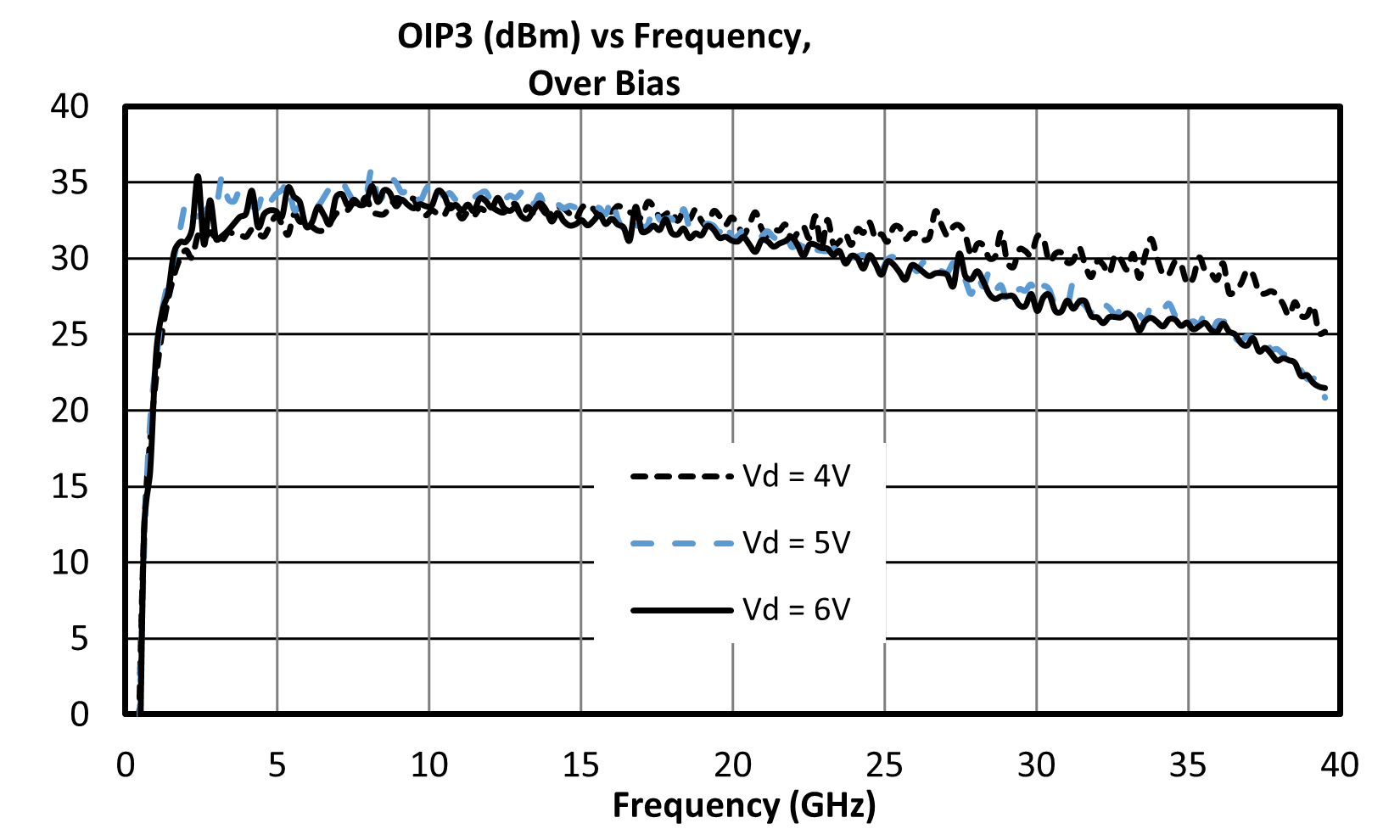
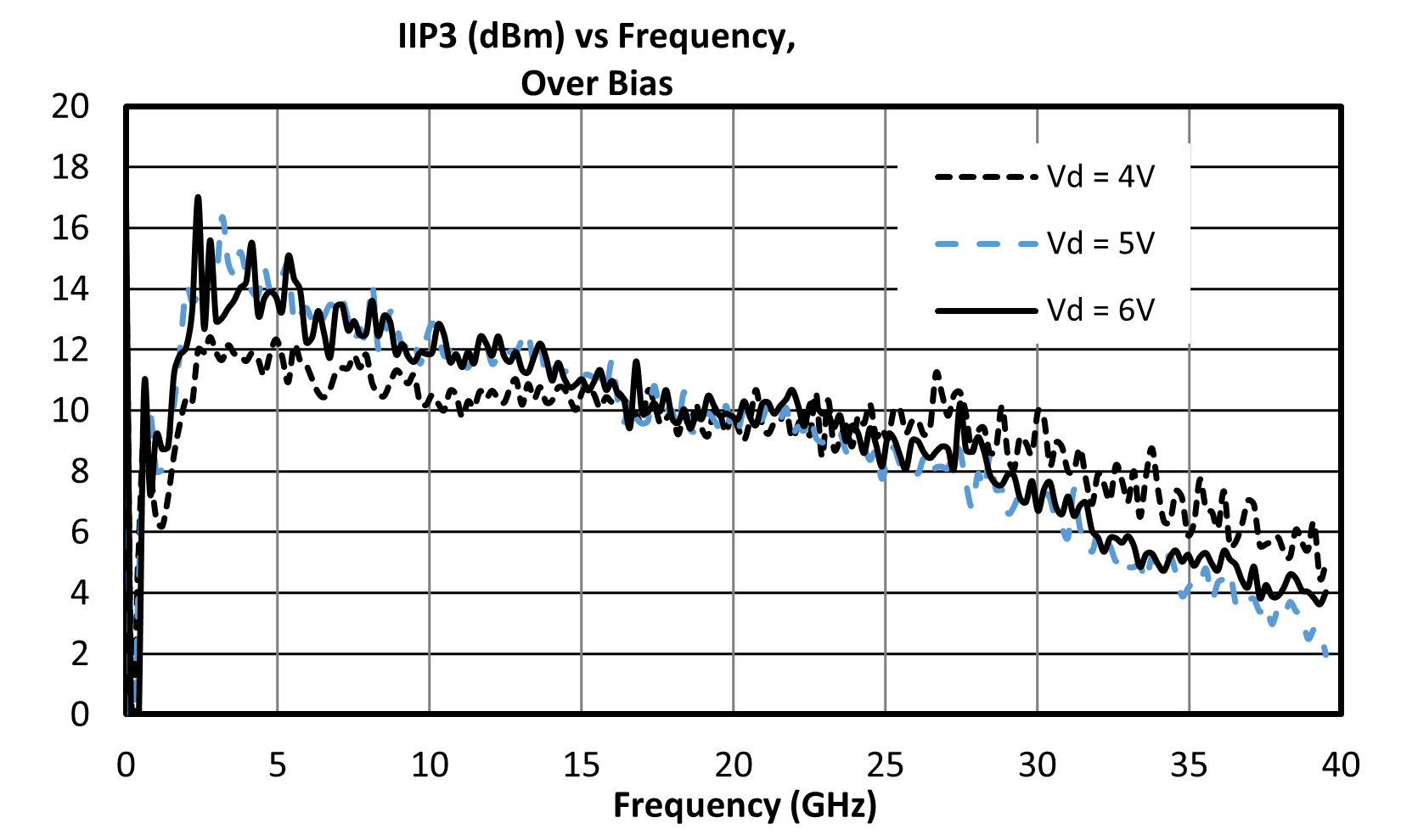
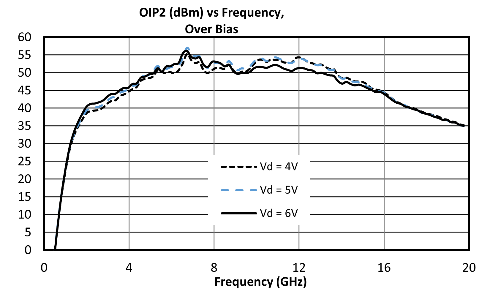
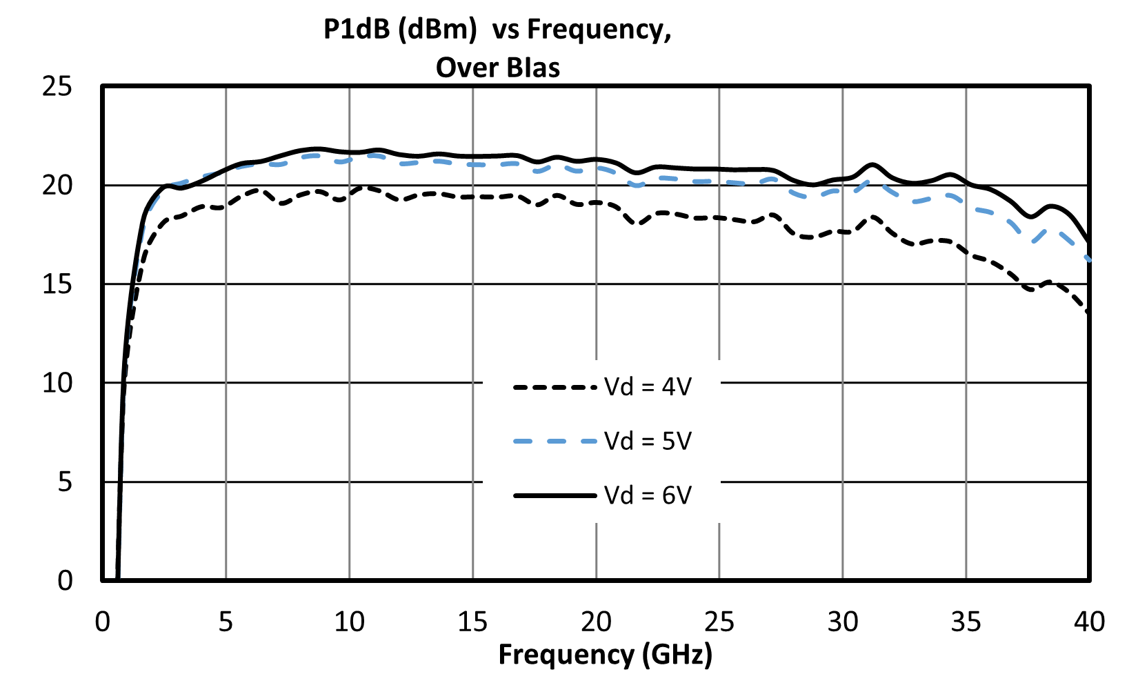
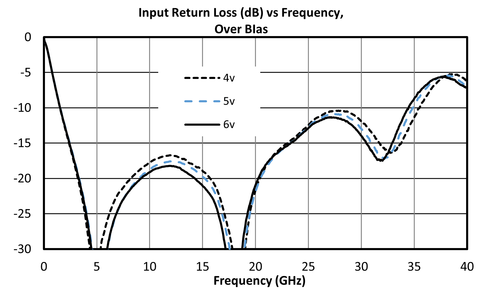
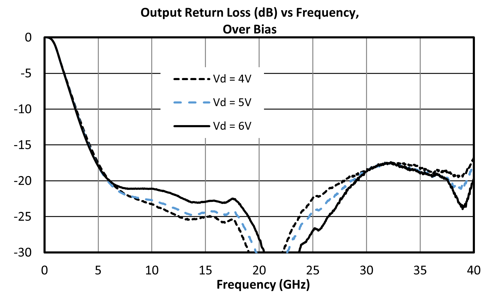
Data taken with gate voltages adjusted to 220 mA Idq.
ADM-8007CH
2 - 40 GHz High Gain Distributed Amplifier, Bare Die
ADM-8007CH
2 - 40 GHz High Gain Distributed Amplifier, Bare Die